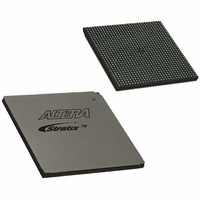
EP1S80B956C7N Altera, EP1S80B956C7N Datasheet - Page 462

EP1S80B956C7N
Manufacturer Part Number
EP1S80B956C7N
Description
IC STRATIX FPGA 80K LE 956-BGA
Manufacturer
Altera
Series
Stratix®r
Datasheet
1.EP1S10F484I6N.pdf
(864 pages)
Specifications of EP1S80B956C7N
Number Of Logic Elements/cells
79040
Number Of Labs/clbs
7904
Total Ram Bits
7427520
Number Of I /o
683
Voltage - Supply
1.425 V ~ 1.575 V
Mounting Type
Surface Mount
Operating Temperature
0°C ~ 85°C
Package / Case
956-BGA
Lead Free Status / RoHS Status
Lead free / RoHS Compliant
Number Of Gates
-
Available stocks
Company
Part Number
Manufacturer
Quantity
Price
- Current page: 462 of 864
- Download datasheet (11Mb)
I/O Pad Placement Guidelines
4–34
Stratix Device Handbook, Volume 2
Thermally enhanced FineLine BGA and
thermally enhanced BGA cavity up
non-thermally enhanced cavity up and
non-thermally enhanced FineLine BGA
Table 4–11. Bidirectional Pad Limitation Formulas (Multiple VREF Inputs & Outputs)
Package Type
The previous equation accounts for the input limitations, but you must
apply the appropriate equation from
limitations.
In addition to the pad placement guidelines, use the following guidelines
when working with V
■
■
Output Enable Group Logic Option in Quartus II
The Quartus II software can check a design to make sure that the pad
placement does not violate the rules mentioned above. When the
software checks the design, if the design contains more bidirectional pins
than what is allowed, the Quartus II software returns a fitting error. When
all the bidirectional pins are either input or output but not both (for
example, in a DDR memory interface), you can use the Output Enable
Group Logic option. Turning on this option directs the Quartus II Fitter
to view the specified nodes as an output enable group. This way, the Fitter
does not violate the requirements for the maximum number of pins
driving out of a V
bidirectional pin is present.
In a design that implements DDR memory interface with dq, dqs and dm
pins utilized, there are two ways to enable the above logic options. You
can enable the logic options through the Assignment Editor or by adding
the following assignments to your project’s ESF file:
OPTIONS_FOR_INDIVIDUAL_NODES_ONLY
{
Each bank can only have a single V
V
share the bank if they have compatible V
for more details).
In all cases listed above, the Quartus II software generates an error
message for illegally placed pads.
dq : OUTPUT_ENABLE_GROUP 1;
dqs : OUTPUT_ENABLE_GROUP 1;
REF
voltage level at a given time. Pins of different I/O standards can
<Total number of bidirectional pads> + <Total number of additional
output pads> 20 (per
<Total number of bidirectional pads> + <Total number of additional
output pads> 15 (per
REF
bank when a voltaged-referenced input pin or
REF
standards:
VREF
VREF
pad)
pad)
Formula
Table 4–9
CCIO
voltage level and a single
CCIO
to determine the output
values (see
Altera Corporation
Table 4–12
June 2006
Related parts for EP1S80B956C7N
Image
Part Number
Description
Manufacturer
Datasheet
Request
R

Part Number:
Description:
CYCLONE II STARTER KIT EP2C20N
Manufacturer:
Altera
Datasheet:

Part Number:
Description:
CPLD, EP610 Family, ECMOS Process, 300 Gates, 16 Macro Cells, 16 Reg., 16 User I/Os, 5V Supply, 35 Speed Grade, 24DIP
Manufacturer:
Altera Corporation
Datasheet:

Part Number:
Description:
CPLD, EP610 Family, ECMOS Process, 300 Gates, 16 Macro Cells, 16 Reg., 16 User I/Os, 5V Supply, 15 Speed Grade, 24DIP
Manufacturer:
Altera Corporation
Datasheet:

Part Number:
Description:
Manufacturer:
Altera Corporation
Datasheet:

Part Number:
Description:
CPLD, EP610 Family, ECMOS Process, 300 Gates, 16 Macro Cells, 16 Reg., 16 User I/Os, 5V Supply, 30 Speed Grade, 24DIP
Manufacturer:
Altera Corporation
Datasheet:

Part Number:
Description:
High-performance, low-power erasable programmable logic devices with 8 macrocells, 10ns
Manufacturer:
Altera Corporation
Datasheet:

Part Number:
Description:
High-performance, low-power erasable programmable logic devices with 8 macrocells, 7ns
Manufacturer:
Altera Corporation
Datasheet:

Part Number:
Description:
Classic EPLD
Manufacturer:
Altera Corporation
Datasheet:

Part Number:
Description:
High-performance, low-power erasable programmable logic devices with 8 macrocells, 10ns
Manufacturer:
Altera Corporation
Datasheet:

Part Number:
Description:
Manufacturer:
Altera Corporation
Datasheet:

Part Number:
Description:
Manufacturer:
Altera Corporation
Datasheet:

Part Number:
Description:
Manufacturer:
Altera Corporation
Datasheet:

Part Number:
Description:
CPLD, EP610 Family, ECMOS Process, 300 Gates, 16 Macro Cells, 16 Reg., 16 User I/Os, 5V Supply, 25 Speed Grade, 24DIP
Manufacturer:
Altera Corporation
Datasheet:


