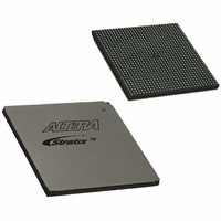
EP1S80B956C7N Altera, EP1S80B956C7N Datasheet - Page 542

EP1S80B956C7N
Manufacturer Part Number
EP1S80B956C7N
Description
IC STRATIX FPGA 80K LE 956-BGA
Manufacturer
Altera
Series
Stratix®r
Datasheet
1.EP1S10F484I6N.pdf
(864 pages)
Specifications of EP1S80B956C7N
Number Of Logic Elements/cells
79040
Number Of Labs/clbs
7904
Total Ram Bits
7427520
Number Of I /o
683
Voltage - Supply
1.425 V ~ 1.575 V
Mounting Type
Surface Mount
Operating Temperature
0°C ~ 85°C
Package / Case
956-BGA
Lead Free Status / RoHS Status
Lead free / RoHS Compliant
Number Of Gates
-
Available stocks
Company
Part Number
Manufacturer
Quantity
Price
- Current page: 542 of 864
- Download datasheet (11Mb)
Software Support
5–70
Stratix Device Handbook, Volume 2
separate the transmitter and receiver in your design, the Quartus II
software merges the fast PLLs when appropriate and gives you the
following message:
Receiver fast PLL <lvds_rx pll name> and transmitter fast PLL
<lvds_tx pll name> are merged together
The Quartus II software gives the following message when it cannot
merge the fast PLLs for the LVDS transmitter and receiver pair in the
design:
tx_outclock Resource
You can use either the global or regional clock for the tx_outclock
signal. If you select Auto in the Quartus II software, the tool uses any
available lines.
SERDES Bypass Mode
You can bypass the SERDES block if your data rate is less than 624 Mbps,
and you must bypass the SERDES block for the
Since you cannot route the fast PLL output to an output pin, you must
create additional DDR I/O circuitry for the transmitter clock output. To
create an
megafunction clocked by the
and datain_l connected to GND.
×1 Mode
For
the Quartus II software that you are using differential signaling.
However, Altera recommends using the DDRIO circuitry when the input
or output data rate is higher than 231 Mbps. The maximum output clock
frequency for
×2 Mode
You must use the DDRIO circuitry for
provides the altddio_in and altddio_out megafunctions to use for
×
×
circuitry in
2 receiver and
2 mode is 624 Mbps.
×
Can't merge transmitter-only fast PLL
<lvds_tx pll name> and receiver-only fast PLL
<lvds_rx pll name>
1 mode, you only need to specify the I/O standard of the pins to tell
×
J transmitter output clock, instantiate an alt_ddio
×
2 mode.
×
1 mode is 420 MHz.
×
2 transmitter, respectively. The maximum data rate in
Figure 5–44
×
J clock with datain_h connected to V
shows the schematic for using DDR
×
2 mode. The Quartus II software
×
1 and
×
Altera Corporation
2 LVDS modules.
July 2005
CC
Related parts for EP1S80B956C7N
Image
Part Number
Description
Manufacturer
Datasheet
Request
R

Part Number:
Description:
CYCLONE II STARTER KIT EP2C20N
Manufacturer:
Altera
Datasheet:

Part Number:
Description:
CPLD, EP610 Family, ECMOS Process, 300 Gates, 16 Macro Cells, 16 Reg., 16 User I/Os, 5V Supply, 35 Speed Grade, 24DIP
Manufacturer:
Altera Corporation
Datasheet:

Part Number:
Description:
CPLD, EP610 Family, ECMOS Process, 300 Gates, 16 Macro Cells, 16 Reg., 16 User I/Os, 5V Supply, 15 Speed Grade, 24DIP
Manufacturer:
Altera Corporation
Datasheet:

Part Number:
Description:
Manufacturer:
Altera Corporation
Datasheet:

Part Number:
Description:
CPLD, EP610 Family, ECMOS Process, 300 Gates, 16 Macro Cells, 16 Reg., 16 User I/Os, 5V Supply, 30 Speed Grade, 24DIP
Manufacturer:
Altera Corporation
Datasheet:

Part Number:
Description:
High-performance, low-power erasable programmable logic devices with 8 macrocells, 10ns
Manufacturer:
Altera Corporation
Datasheet:

Part Number:
Description:
High-performance, low-power erasable programmable logic devices with 8 macrocells, 7ns
Manufacturer:
Altera Corporation
Datasheet:

Part Number:
Description:
Classic EPLD
Manufacturer:
Altera Corporation
Datasheet:

Part Number:
Description:
High-performance, low-power erasable programmable logic devices with 8 macrocells, 10ns
Manufacturer:
Altera Corporation
Datasheet:

Part Number:
Description:
Manufacturer:
Altera Corporation
Datasheet:

Part Number:
Description:
Manufacturer:
Altera Corporation
Datasheet:

Part Number:
Description:
Manufacturer:
Altera Corporation
Datasheet:

Part Number:
Description:
CPLD, EP610 Family, ECMOS Process, 300 Gates, 16 Macro Cells, 16 Reg., 16 User I/Os, 5V Supply, 25 Speed Grade, 24DIP
Manufacturer:
Altera Corporation
Datasheet:


