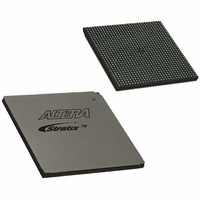
EP1S80B956C7N Altera, EP1S80B956C7N Datasheet - Page 485

EP1S80B956C7N
Manufacturer Part Number
EP1S80B956C7N
Description
IC STRATIX FPGA 80K LE 956-BGA
Manufacturer
Altera
Series
Stratix®r
Datasheet
1.EP1S10F484I6N.pdf
(864 pages)
Specifications of EP1S80B956C7N
Number Of Logic Elements/cells
79040
Number Of Labs/clbs
7904
Total Ram Bits
7427520
Number Of I /o
683
Voltage - Supply
1.425 V ~ 1.575 V
Mounting Type
Surface Mount
Operating Temperature
0°C ~ 85°C
Package / Case
956-BGA
Lead Free Status / RoHS Status
Lead free / RoHS Compliant
Number Of Gates
-
Available stocks
Company
Part Number
Manufacturer
Quantity
Price
- Current page: 485 of 864
- Download datasheet (11Mb)
Figure 5–8. High-Speed 1-to-1 Transmitter Clock Output
Note to
(1)
Using SERDES
to Implement
DDR
Altera Corporation
July 2005
This figure does not show additional circuitry for clock or data manipulation.
Figure
Logic Array
Stratix
5–8:
Some designs require a 2-to-1 data-to-clock ratio. These systems are
usually based on Rapid I/O, SPI-4 Phase 2 (POS_PHY Level 4), or
HyperTransport interfaces, and support various data rates. Stratix
devices meet this requirement for such applications by providing a
variable clock division factor. The SERDES clock division factor is set to 2
for double data rate (DDR).
An additional differential channel (as described in
Output” on page
transmitter clock output signal with half the frequency of the data.
For example, when a system is required to transmit 6.4 Gbps with a
2-to-1 clock-to-data ratio, program the SERDES with eight high-speed
channels running at 800 Mbps each. When you set the output clock
division factor (2 for this example), the Quartus II software automatically
assigns a ninth channel as the transmitter clock output. You can edge- or
center-align the transmitter clock by selecting the default PLL phase or
selecting the negative-edge transmitter clock output. On the receiver side,
the clock signal is connected to the receiver PLL's clock.
The multiplication factor W is also calculated automatically. The data rate
divides by the input clock frequency to calculate the W factor. The
deserialization factor (J) may be 4, 7, 8, or 10.
Transmitter Circuit
PD9
PD8
PD7
PD6
PD5
PD4
PD3
PD2
PD0
PD1
PLL (1)
Fast
Register
Parallel
TXLOADEN
× W
5–10) is automatically configured to produce the
PD9
PD8
PD7
PD6
PD5
PD4
PD3
PD2
PD1
PD0
High-Speed Differential I/O Interfaces in Stratix Devices
Register
Serial
Stratix Device Handbook, Volume 2
Inverter
“Transmitter Clock
TXOUT+
TXOUT−
5–13
Related parts for EP1S80B956C7N
Image
Part Number
Description
Manufacturer
Datasheet
Request
R

Part Number:
Description:
CYCLONE II STARTER KIT EP2C20N
Manufacturer:
Altera
Datasheet:

Part Number:
Description:
CPLD, EP610 Family, ECMOS Process, 300 Gates, 16 Macro Cells, 16 Reg., 16 User I/Os, 5V Supply, 35 Speed Grade, 24DIP
Manufacturer:
Altera Corporation
Datasheet:

Part Number:
Description:
CPLD, EP610 Family, ECMOS Process, 300 Gates, 16 Macro Cells, 16 Reg., 16 User I/Os, 5V Supply, 15 Speed Grade, 24DIP
Manufacturer:
Altera Corporation
Datasheet:

Part Number:
Description:
Manufacturer:
Altera Corporation
Datasheet:

Part Number:
Description:
CPLD, EP610 Family, ECMOS Process, 300 Gates, 16 Macro Cells, 16 Reg., 16 User I/Os, 5V Supply, 30 Speed Grade, 24DIP
Manufacturer:
Altera Corporation
Datasheet:

Part Number:
Description:
High-performance, low-power erasable programmable logic devices with 8 macrocells, 10ns
Manufacturer:
Altera Corporation
Datasheet:

Part Number:
Description:
High-performance, low-power erasable programmable logic devices with 8 macrocells, 7ns
Manufacturer:
Altera Corporation
Datasheet:

Part Number:
Description:
Classic EPLD
Manufacturer:
Altera Corporation
Datasheet:

Part Number:
Description:
High-performance, low-power erasable programmable logic devices with 8 macrocells, 10ns
Manufacturer:
Altera Corporation
Datasheet:

Part Number:
Description:
Manufacturer:
Altera Corporation
Datasheet:

Part Number:
Description:
Manufacturer:
Altera Corporation
Datasheet:

Part Number:
Description:
Manufacturer:
Altera Corporation
Datasheet:

Part Number:
Description:
CPLD, EP610 Family, ECMOS Process, 300 Gates, 16 Macro Cells, 16 Reg., 16 User I/Os, 5V Supply, 25 Speed Grade, 24DIP
Manufacturer:
Altera Corporation
Datasheet:


