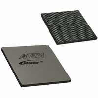
EP1S80B956C7N Altera, EP1S80B956C7N Datasheet - Page 844

EP1S80B956C7N
Manufacturer Part Number
EP1S80B956C7N
Description
IC STRATIX FPGA 80K LE 956-BGA
Manufacturer
Altera
Series
Stratix®r
Datasheet
1.EP1S10F484I6N.pdf
(864 pages)
Specifications of EP1S80B956C7N
Number Of Logic Elements/cells
79040
Number Of Labs/clbs
7904
Total Ram Bits
7427520
Number Of I /o
683
Voltage - Supply
1.425 V ~ 1.575 V
Mounting Type
Surface Mount
Operating Temperature
0°C ~ 85°C
Package / Case
956-BGA
Lead Free Status / RoHS Status
Lead free / RoHS Compliant
Number Of Gates
-
Available stocks
Company
Part Number
Manufacturer
Quantity
Price
- Current page: 844 of 864
- Download datasheet (11Mb)
Voltage Regulators
14–4
Stratix Device Handbook, Volume 2
Input voltage range (V
Line regulation
(line regulation, V
Load regulation
(load regulation, V
Output voltage selection
Quiescent current
Dropout voltage
Current limiting
Thermal overload protection
Reverse current protection
Stability
Table 14–2. Voltage Regulator Specifications & Terminology (Part 1 of 2)
Specification/Terminology
OUT
OUT
)
)
IN
,V
CC
)
Table 14–2
encountered with voltage regulators. Symbols are shown in parentheses.
If the symbols are different for linear and switching regulators, the linear
regulator symbol is listed first.
Minimum and maximum input voltages define the input voltage range, which
is determined by the regulator process voltage capabilities.
Line regulation is the variation of the output voltage (V
the input voltage (V
impedance all influence line regulation. Higher gain results in better
regulation. Board layout and regulator pin-outs are also important because
stray resistance can introduce errors.
Load regulation is a variation in the output voltage caused by changes in the
input supply current. Linear Technology regulators are designed to minimize
load regulation, which is affected by error amplifier gain, pass transistor gain,
and output impedance.
Output voltage selection is adjustable by resistor voltage divider networks,
connected to the error amplifier input, that control the output voltage. There
are multiple output regulators that create 5.0-, 3.3-, 2.5-, 1.8- and 1.5-V
supplies.
Quiescent current is the supply current during no-load or quiescent state.
This current is sometimes used as a general term for a supply current used
by the regulator.
Dropout voltage is the difference between the input and output voltages
when the input is low enough to cause the output to drop out of regulation.
The dropout voltage should be as low as possible for better efficiency.
Voltage regulators are designed to limit the amount of output current in the
event of a failing load. A short in the load causes the output current and
voltage to decrease. This event cuts power dissipation in the regulator during
a short circuit.
This feature limits power dissipation if the regulator overheats. When a
specified temperature is reached, the regulator turns off the output drive
transistors, allowing the regulator to cool. Normal operation resumes once
the regulator reaches a normal operating temperature.
If the input power supply fails, large output capacitors can cause a substantial
reverse current to flow backward through the regulator, potentially causing
damage. To prevent damage, protection diodes in the regulator create a path
for the current to flow from V
The dominant pole placed by the output capacitor influences stability.
Voltage regulator vendors can assist you in output capacitor selection for
regulator designs that differ from what is offered.
shows the terminology and specifications commonly
IN
). Error amplifier gain, pass transistor gain, and output
OUT
Description
to V
IN
.
OUT
Altera Corporation
) with changes in
January 2005
Related parts for EP1S80B956C7N
Image
Part Number
Description
Manufacturer
Datasheet
Request
R

Part Number:
Description:
CYCLONE II STARTER KIT EP2C20N
Manufacturer:
Altera
Datasheet:

Part Number:
Description:
CPLD, EP610 Family, ECMOS Process, 300 Gates, 16 Macro Cells, 16 Reg., 16 User I/Os, 5V Supply, 35 Speed Grade, 24DIP
Manufacturer:
Altera Corporation
Datasheet:

Part Number:
Description:
CPLD, EP610 Family, ECMOS Process, 300 Gates, 16 Macro Cells, 16 Reg., 16 User I/Os, 5V Supply, 15 Speed Grade, 24DIP
Manufacturer:
Altera Corporation
Datasheet:

Part Number:
Description:
Manufacturer:
Altera Corporation
Datasheet:

Part Number:
Description:
CPLD, EP610 Family, ECMOS Process, 300 Gates, 16 Macro Cells, 16 Reg., 16 User I/Os, 5V Supply, 30 Speed Grade, 24DIP
Manufacturer:
Altera Corporation
Datasheet:

Part Number:
Description:
High-performance, low-power erasable programmable logic devices with 8 macrocells, 10ns
Manufacturer:
Altera Corporation
Datasheet:

Part Number:
Description:
High-performance, low-power erasable programmable logic devices with 8 macrocells, 7ns
Manufacturer:
Altera Corporation
Datasheet:

Part Number:
Description:
Classic EPLD
Manufacturer:
Altera Corporation
Datasheet:

Part Number:
Description:
High-performance, low-power erasable programmable logic devices with 8 macrocells, 10ns
Manufacturer:
Altera Corporation
Datasheet:

Part Number:
Description:
Manufacturer:
Altera Corporation
Datasheet:

Part Number:
Description:
Manufacturer:
Altera Corporation
Datasheet:

Part Number:
Description:
Manufacturer:
Altera Corporation
Datasheet:

Part Number:
Description:
CPLD, EP610 Family, ECMOS Process, 300 Gates, 16 Macro Cells, 16 Reg., 16 User I/Os, 5V Supply, 25 Speed Grade, 24DIP
Manufacturer:
Altera Corporation
Datasheet:


