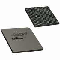
EP1S80B956C7N Altera, EP1S80B956C7N Datasheet - Page 689

EP1S80B956C7N
Manufacturer Part Number
EP1S80B956C7N
Description
IC STRATIX FPGA 80K LE 956-BGA
Manufacturer
Altera
Series
Stratix®r
Datasheet
1.EP1S10F484I6N.pdf
(864 pages)
Specifications of EP1S80B956C7N
Number Of Logic Elements/cells
79040
Number Of Labs/clbs
7904
Total Ram Bits
7427520
Number Of I /o
683
Voltage - Supply
1.425 V ~ 1.575 V
Mounting Type
Surface Mount
Operating Temperature
0°C ~ 85°C
Package / Case
956-BGA
Lead Free Status / RoHS Status
Lead free / RoHS Compliant
Number Of Gates
-
Available stocks
Company
Part Number
Manufacturer
Quantity
Price
- Current page: 689 of 864
- Download datasheet (11Mb)
Altera Corporation
July 2005
Architectural Element Names
The architectural element naming system within Stratix and Stratix GX
devices differs from the row-column coordinate system (for example,
LC1_A2, LAB_B1) used in previous Altera device families. Stratix and
Stratix GX devices uses a new naming system based on the X-Y
coordinate system, (X, Y). A number (N) designates the location within the
block where the logic resides, such as LEs within an LAB. Because the
Stratix and Stratix GX architectures are column-based, this naming
simplifies location assignments. Stratix and Stratix GX architectural
blocks include:
■
■
■
■
■
■
Elements within architectural blocks include:
■
■
■
■
■
■
LAB: logic array block
DSP: digital signal processing block
DSPOUT: adder/subtractor/accumulator or summation block of the
DSP block
M512: 512-bit memory block
M4K: 4-Kbit memory block
M-RAM: 512-Kbit memory block
LE: logic element
IOC: I/O element
PLL: phase-locked loop
DSPMULT: DSP block multiplier
SERDESTX: transmitter serializer/deserializer
SERDESRX: receiver serializer/deserializer
Transitioning APEX Designs to Stratix & Stratix GX Devices
Stratix Device Handbook, Volume 2
10–5
Related parts for EP1S80B956C7N
Image
Part Number
Description
Manufacturer
Datasheet
Request
R

Part Number:
Description:
CYCLONE II STARTER KIT EP2C20N
Manufacturer:
Altera
Datasheet:

Part Number:
Description:
CPLD, EP610 Family, ECMOS Process, 300 Gates, 16 Macro Cells, 16 Reg., 16 User I/Os, 5V Supply, 35 Speed Grade, 24DIP
Manufacturer:
Altera Corporation
Datasheet:

Part Number:
Description:
CPLD, EP610 Family, ECMOS Process, 300 Gates, 16 Macro Cells, 16 Reg., 16 User I/Os, 5V Supply, 15 Speed Grade, 24DIP
Manufacturer:
Altera Corporation
Datasheet:

Part Number:
Description:
Manufacturer:
Altera Corporation
Datasheet:

Part Number:
Description:
CPLD, EP610 Family, ECMOS Process, 300 Gates, 16 Macro Cells, 16 Reg., 16 User I/Os, 5V Supply, 30 Speed Grade, 24DIP
Manufacturer:
Altera Corporation
Datasheet:

Part Number:
Description:
High-performance, low-power erasable programmable logic devices with 8 macrocells, 10ns
Manufacturer:
Altera Corporation
Datasheet:

Part Number:
Description:
High-performance, low-power erasable programmable logic devices with 8 macrocells, 7ns
Manufacturer:
Altera Corporation
Datasheet:

Part Number:
Description:
Classic EPLD
Manufacturer:
Altera Corporation
Datasheet:

Part Number:
Description:
High-performance, low-power erasable programmable logic devices with 8 macrocells, 10ns
Manufacturer:
Altera Corporation
Datasheet:

Part Number:
Description:
Manufacturer:
Altera Corporation
Datasheet:

Part Number:
Description:
Manufacturer:
Altera Corporation
Datasheet:

Part Number:
Description:
Manufacturer:
Altera Corporation
Datasheet:

Part Number:
Description:
CPLD, EP610 Family, ECMOS Process, 300 Gates, 16 Macro Cells, 16 Reg., 16 User I/Os, 5V Supply, 25 Speed Grade, 24DIP
Manufacturer:
Altera Corporation
Datasheet:


