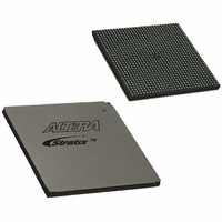
EP1S80B956C7N Altera, EP1S80B956C7N Datasheet - Page 502

EP1S80B956C7N
Manufacturer Part Number
EP1S80B956C7N
Description
IC STRATIX FPGA 80K LE 956-BGA
Manufacturer
Altera
Series
Stratix®r
Datasheet
1.EP1S10F484I6N.pdf
(864 pages)
Specifications of EP1S80B956C7N
Number Of Logic Elements/cells
79040
Number Of Labs/clbs
7904
Total Ram Bits
7427520
Number Of I /o
683
Voltage - Supply
1.425 V ~ 1.575 V
Mounting Type
Surface Mount
Operating Temperature
0°C ~ 85°C
Package / Case
956-BGA
Lead Free Status / RoHS Status
Lead free / RoHS Compliant
Number Of Gates
-
Available stocks
Company
Part Number
Manufacturer
Quantity
Price
- Current page: 502 of 864
- Download datasheet (11Mb)
Source-Synchronous Timing Budget
Source-
Synchronous
Timing Budget
5–30
Stratix Device Handbook, Volume 2
■
■
■
■
This section discusses the timing budget, waveforms, and specifications
for source-synchronous signaling in Stratix devices. LVDS, LVPECL,
PCML, and HyperTransport I/O standards enable high-speed data
transmission. This high data-transmission rate results in better overall
system performance. To take advantage of fast system performance, you
must understand how to analyze timing for these high-speed signals.
Timing analysis for the differential block is different from traditional
synchronous timing analysis techniques.
Rather than focusing on clock-to-output and setup times, source-
synchronous timing analysis is based on the skew between the data and
the clock signals. High-speed differential data transmission requires you
to use timing parameters provided by IC vendors and to consider board
skew, cable skew, and clock jitter. This section defines the source-
synchronous differential data orientation timing parameters, and timing
budget definitions for Stratix devices, and explains how to use these
timing parameters to determine a design's maximum performance.
Differential Data Orientation
There is a set relationship between an external clock and the incoming
data. For operation at 840 Mbps and W = 10, the external clock is
multiplied by 10 and phase-aligned by the PLL to coincide with the
sampling window of each data bit. The third falling edge of high-
frequency clock is used to strobe the incoming high-speed data.
Therefore, the first two bits belong to the previous cycle.
shows the data bit orientation of the ×10 mode as defined in the
Quartus II software.
After the pattern detection state machine, use another synchronizing
register to capture the generated SYNC signal and synchronize it to
the
Since the skew in the path from the output of this synchronizing
register to the PLL is undefined, the state machine must generate a
pulse that is high for two
Since the SYNC generator circuitry only generates a single fast clock
period pulse for each SYNC pulse, you cannot generate additional
SYNC pulses until the comparator signal is reset low.
To guarantee the pattern detection state machine does not incorrectly
generate multiple SYNC pulses to shift a single bit, the state machine
must hold the SYNC signal low for at least three
between pulses.
×
1 clock.
×
1 clock periods.
×
1 clock periods
Altera Corporation
Figure 5–23
July 2005
Related parts for EP1S80B956C7N
Image
Part Number
Description
Manufacturer
Datasheet
Request
R

Part Number:
Description:
CYCLONE II STARTER KIT EP2C20N
Manufacturer:
Altera
Datasheet:

Part Number:
Description:
CPLD, EP610 Family, ECMOS Process, 300 Gates, 16 Macro Cells, 16 Reg., 16 User I/Os, 5V Supply, 35 Speed Grade, 24DIP
Manufacturer:
Altera Corporation
Datasheet:

Part Number:
Description:
CPLD, EP610 Family, ECMOS Process, 300 Gates, 16 Macro Cells, 16 Reg., 16 User I/Os, 5V Supply, 15 Speed Grade, 24DIP
Manufacturer:
Altera Corporation
Datasheet:

Part Number:
Description:
Manufacturer:
Altera Corporation
Datasheet:

Part Number:
Description:
CPLD, EP610 Family, ECMOS Process, 300 Gates, 16 Macro Cells, 16 Reg., 16 User I/Os, 5V Supply, 30 Speed Grade, 24DIP
Manufacturer:
Altera Corporation
Datasheet:

Part Number:
Description:
High-performance, low-power erasable programmable logic devices with 8 macrocells, 10ns
Manufacturer:
Altera Corporation
Datasheet:

Part Number:
Description:
High-performance, low-power erasable programmable logic devices with 8 macrocells, 7ns
Manufacturer:
Altera Corporation
Datasheet:

Part Number:
Description:
Classic EPLD
Manufacturer:
Altera Corporation
Datasheet:

Part Number:
Description:
High-performance, low-power erasable programmable logic devices with 8 macrocells, 10ns
Manufacturer:
Altera Corporation
Datasheet:

Part Number:
Description:
Manufacturer:
Altera Corporation
Datasheet:

Part Number:
Description:
Manufacturer:
Altera Corporation
Datasheet:

Part Number:
Description:
Manufacturer:
Altera Corporation
Datasheet:

Part Number:
Description:
CPLD, EP610 Family, ECMOS Process, 300 Gates, 16 Macro Cells, 16 Reg., 16 User I/Os, 5V Supply, 25 Speed Grade, 24DIP
Manufacturer:
Altera Corporation
Datasheet:


