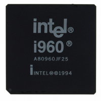
A80960JF3V25 Intel, A80960JF3V25 Datasheet - Page 11

A80960JF3V25
Manufacturer Part Number
A80960JF3V25
Description
IC MPU I960JF 3.3V 25MHZ 132-PGA
Manufacturer
Intel
Datasheet
1.NG80960JC66.pdf
(86 pages)
Specifications of A80960JF3V25
Processor Type
i960
Features
JF suffix, 32-Bit, 4K Cache
Speed
25MHz
Voltage
3.3V
Mounting Type
Surface Mount
Package / Case
132-PGA
Lead Free Status / RoHS Status
Lead free / RoHS Compliant
Other names
819540
Available stocks
Company
Part Number
Manufacturer
Quantity
Price
Company:
Part Number:
A80960JF3V25
Manufacturer:
Intel
Quantity:
135
2.2
2.3
2.4
Datasheet
Burst Bus
A 32-bit high-performance Bus Controller Unit (BCU) interfaces the 80960Jx to external memory
and peripherals. The BCU fetches instructions and transfers data at the rate of up to four 32-bit
words per six clock cycles. The external address/data bus is multiplexed.
Users may configure the 80960Jx’s bus controller to match an application’s fundamental memory
organization. Physical bus width is register-programmed for up to eight regions. Byte ordering and
data caching are programmed through a group of logical memory templates and a defaults register.
The BCU’s features include:
Upon reset, the 80960Jx conducts an internal self-test. Then, before executing its first instruction, it
performs an external bus confidence test by performing a checksum on the first words of the
initialization boot record (IBR).
Timer Unit
The timer unit (TU) contains two independent 32-bit timers that are capable of counting at several
clock rates and generating interrupts. Each is programmed by use of the TU registers. These
memory-mapped registers are addressable on 32-bit boundaries. The timers have a single-shot
mode and auto-reload capabilities for continuous operation. Each timer has an independent
interrupt request to the 80960Jx’s interrupt controller. The TU may generate a fault when
unauthorized writes from user mode are detected. Clock prescaling is supported.
Priority Interrupt Controller
A programmable interrupt controller manages up to 240 external sources through an 8-bit external
interrupt port. Alternatively, the interrupt inputs may be configured for individual edge- or level-
triggered inputs. The interrupt unit (IU) also accepts interrupts from the two on-chip timer channels
and a single Non-Maskable Interrupt (NMI#) pin. Interrupts are serviced according to their priority
levels relative to the current process priority.
Low interrupt latency is critical to many embedded applications. As part of its highly flexible
interrupt mechanism, the 80960Jx exploits several techniques to minimize latency:
•
•
•
•
•
•
•
•
•
•
Multiplexed external bus to minimize pin count
32-, 16-, and 8-bit bus widths to simplify I/O interfaces
External ready control for address-to-data, data-to-data and data-to-next-address wait state
types
Support for big or little endian byte ordering to facilitate the porting of existing program code
Unaligned bus accesses performed transparently
Three-deep load/store queue to decouple the bus from the core
Interrupt vectors and interrupt handler routines may be reserved on-chip.
Register frames for high-priority interrupt handlers may be cached on-chip.
The interrupt stack may be placed in cacheable memory space.
Interrupt microcode executes at two or three times the bus frequency for the 80960JD/JC and
80960JT, respectively.
80960JA/JF/JD/JS/JC/JT 3.3 V Embedded 32-Bit Microprocessor
11


