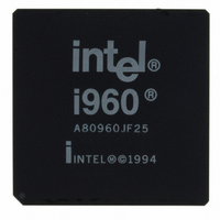
A80960JF3V25 Intel, A80960JF3V25 Datasheet - Page 36

A80960JF3V25
Manufacturer Part Number
A80960JF3V25
Description
IC MPU I960JF 3.3V 25MHZ 132-PGA
Manufacturer
Intel
Datasheet
1.NG80960JC66.pdf
(86 pages)
Specifications of A80960JF3V25
Processor Type
i960
Features
JF suffix, 32-Bit, 4K Cache
Speed
25MHz
Voltage
3.3V
Mounting Type
Surface Mount
Package / Case
132-PGA
Lead Free Status / RoHS Status
Lead free / RoHS Compliant
Other names
819540
Available stocks
Company
Part Number
Manufacturer
Quantity
Price
Company:
Part Number:
A80960JF3V25
Manufacturer:
Intel
Quantity:
135
80960JA/JF/JD/JS/JC/JT 3.3 V Embedded 32-Bit Microprocessor
4.3
4.4
36
Figure 8. VCC5 Current-Limiting Resistor
Note: Pins identified as NC must not be connected in the system.
Connection Recommendations
For clean on-chip power distribution, V
units. Power and ground connections must be made to all 80960Jx power and ground pins. On the
circuit board, every V
a ground plane. Place liberal decoupling capacitance near the 80960Jx, since the processor may
cause transient power surges.
The 80960JS/JC/JT processors are produced on Intel’s advanced CMOS process. Proper bulk
decoupling must be used to prevent device damage during initial power up and during transitions
from low power mode to normal processor operation. Power supply behavior during these
transitions may cause the power supply to exceed the maximum V
device damage.
Pay special attention to the Test Reset (TRST#) pin. It is essential that the JTAG Boundary Scan
Test Access Port (TAP) controller initializes to a known state whether it may be used or not. When
the JTAG Boundary Scan function may be used, connect a pull-down resistor between the TRST#
pin and V
testing), connect the TRST# pin to V
Do not connect the TDI, TDO, and TCK pins when the TAP Controller may not be used.
VCC5 Pin Requirements (VDIFF)
In 3.3 V only systems where the 80960Jx input pins are driven from 3.3 V logic, connect the VCC5
pin directly to the 3.3 V V
In mixed voltage systems where the processor is powered by 3.3 V and interfaces with 5 V
components, VCC5 must be connected to 5 V. This allows proper 5 V tolerant buffer operation, and
prevents damage to the input pins. The voltage differential between the 80960Jx VCC5 pin and its
3.3 V V
pin may exceed the value at which the processor is damaged. Instances when the voltage may
exceed 2.25 V is during power up or power down, where one source reaches its level faster than the
other, briefly causing an excess voltage differential. Another instance is during steady-state
operation, where the differential voltage of the regulator (provided a regulator is used) cannot be
maintained within 2.25 V. Two methods are possible to prevent this from happening:
•
•
Use a regulator that is designed to prevent the voltage differential from exceeding 2.25 V.
or:
As shown in
through VCC5.
+5 V (±0.25 V)
CC
SS
pins must not exceed 2.25 V. When this requirement is not met, current flow through the
. When the JTAG Boundary Scan function may not be used (even for board-level
Figure
(±5%, 0.5 W)
CC
100
8, place a 100
pin should connect to a power plane and every V
CC
plane.
VCC5 Pin
SS
.
CC
resistor in series with the VCC5 pin to limit the current
and V
SS
pins separately feed the device’s functional
CC
specification and may cause
SS
pin should connect to
Datasheet


