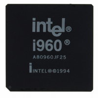
A80960JF3V25 Intel, A80960JF3V25 Datasheet - Page 19

A80960JF3V25
Manufacturer Part Number
A80960JF3V25
Description
IC MPU I960JF 3.3V 25MHZ 132-PGA
Manufacturer
Intel
Datasheet
1.NG80960JC66.pdf
(86 pages)
Specifications of A80960JF3V25
Processor Type
i960
Features
JF suffix, 32-Bit, 4K Cache
Speed
25MHz
Voltage
3.3V
Mounting Type
Surface Mount
Package / Case
132-PGA
Lead Free Status / RoHS Status
Lead free / RoHS Compliant
Other names
819540
Available stocks
Company
Part Number
Manufacturer
Quantity
Price
Company:
Part Number:
A80960JF3V25
Manufacturer:
Intel
Quantity:
135
Datasheet
Table 8. Pin Description—External Bus Signals (Sheet 2 of 4)
HLTD[1:0]
BE[3:0]#
WIDTH/
NAME
DT/R#
W/R#
D/C#
TYPE
R(X)
P(Q)
P(Q)
P(Q)
R(1)
H(Z)
R(0)
H(Z)
H(Z)
R(0)
H(Z)
R(0)
H(Z)
P(1)
P(1)
O
O
O
O
O
80960JA/JF/JD/JS/JC/JT 3.3 V Embedded 32-Bit Microprocessor
BYTE ENABLES select which of up to four data bytes on the bus participate in the
current bus access. Byte enable encoding is dependent on the bus width of the
memory region accessed:
32-bit bus:
16-bit bus:
8-bit bus:
The processor asserts byte enables, byte high enable and byte low enable during
Since unaligned bus requests are split into separate bus transactions, these signals
do not toggle during a burst. They remain active through the last T
For accesses to 8- and 16-bit memory, the processor asserts the address bits in
conjunction with A[3:2] described above.
WIDTH/HALTED signals denote the physical memory attributes for a bus
transaction:
WIDTH/
HLTD1
0
0
1
1
The processor floats the WIDTH/HLTD pins whenever it relinquishes the bus in
response to a HOLD request, regardless of prior operating state.
DATA/CODE indicates that a bus access is a data access (1) or an instruction
access (0). D/C# has the same timing as W/R#.
0 = instruction access
1 = data access
WRITE/READ specifies, during a
read (0). It is latched on-chip and remains valid during T
0 = read
1 = write
DATA TRANSMIT / RECEIVE indicates the direction of data transfer to and from the
address/data bus. It is low during T
and T
0 = receive
1 = transmit
BE3# enables data on AD[31:24]
BE2# enables data on AD[23:16]
BE1# enables data on AD[15:8]
BE0# enables data on AD[7:0]
BE3# becomes Byte High Enable (enables data on AD[15:8])
BE2# is not used (state is high)
BE1# becomes Address Bit 1 (A1)
BE0# becomes Byte Low Enable (enables data on AD[7:0])
BE3# is not used (state is high)
BE2# is not used (state is high)
BE1# becomes Address Bit 1 (A1)
BE0# becomes Address Bit 0 (A0)
w
/T
d
cycles for a write. DT/R# never changes state when DEN# is asserted.
WIDTH/
HLTD0
0
1
0
1
8 Bits Wide
16 Bits Wide
32 Bits Wide
Processor Halted
T
DESCRIPTION
a
a
cycle, whether the operation is a write (1) or
and T
w
/T
d
cycles for a read; it is high during
d
cycles.
d
cycle.
T
T
a
a
19
.


