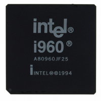
A80960JF3V25 Intel, A80960JF3V25 Datasheet - Page 20

A80960JF3V25
Manufacturer Part Number
A80960JF3V25
Description
IC MPU I960JF 3.3V 25MHZ 132-PGA
Manufacturer
Intel
Datasheet
1.NG80960JC66.pdf
(86 pages)
Specifications of A80960JF3V25
Processor Type
i960
Features
JF suffix, 32-Bit, 4K Cache
Speed
25MHz
Voltage
3.3V
Mounting Type
Surface Mount
Package / Case
132-PGA
Lead Free Status / RoHS Status
Lead free / RoHS Compliant
Other names
819540
Available stocks
Company
Part Number
Manufacturer
Quantity
Price
Company:
Part Number:
A80960JF3V25
Manufacturer:
Intel
Quantity:
135
80960JA/JF/JD/JS/JC/JT 3.3 V Embedded 32-Bit Microprocessor
20
Table 8.
Pin Description—External Bus Signals (Sheet 3 of 4)
RDYRCV#
BLAST#
LOCK#/
ONCE#
NAME
HOLD
DEN#
TYPE
R(H)
R(1)
H(Z)
P(1)
R(1)
H(Z)
P(1)
S(L)
S(L)
H(Z)
P(1)
S(L)
I/O
O
O
I
I
DATA ENABLE indicates data transfer cycles during a bus access. DEN# is
asserted at the start of the first data cycle in a bus access and deasserted at the end
of the last data cycle. DEN# is used with DT/R# to provide control for data
transceivers connected to the data bus.
0 = data cycle
1 = not data cycle
BURST LAST indicates the last transfer in a bus access. BLAST# is asserted in the
last data transfer of burst and non-burst accesses. BLAST# remains active as long
as wait states are inserted through the RDYRCV# pin. BLAST# becomes inactive
after the final data transfer in a bus cycle.
0 = last data transfer
1 = not last data transfer
READY/RECOVER indicates that data on AD lines may be sampled or removed.
When RDYRCV# is not asserted during a T
next cycle by inserting a wait state (T
0 = sample data
1 = don’t sample data
The RDYRCV# pin has another function during the recovery (T
processor continues to insert additional recovery states until it samples the pin
HIGH. This function gives slow external devices more time to float their buffers
before the processor begins to drive address again.
0 = insert wait states
1 = recovery complete
BUS LOCK indicates that an atomic read-modify-write operation is in progress. The
LOCK# output is asserted in the first clock of an atomic operation and deasserted in
the last data transfer of the sequence. The processor does not grant HOLDA while it
is asserting LOCK#. This prevents external agents from accessing memory involved
in semaphore operations.
0 = Atomic read-modify-write in progress
1 = Atomic read-modify-write not in progress
ONCE MODE: The processor samples the ONCE# input during reset. When it is
asserted LOW at the end of reset, the processor enters ONCE mode. In ONCE
mode, the processor stops all clocks and floats all output pins. The pin has a weak
internal pullup which is active during reset to ensure normal operation when the pin
is left unconnected.
0 = ONCE mode enabled
1 = ONCE mode not enabled
HOLD: A request from an external bus master to acquire the bus. When the
processor receives HOLD and grants bus control to another master, it asserts
HOLDA, floats the address/data and control lines and enters the T
HOLD is deasserted, the processor deasserts HOLDA and enters either the T
state, resuming control of the address/data and control lines.
0 = no hold request
1 = hold request
DESCRIPTION
w
).
d
cycle, the T
d
cycle is extended to the
r
) state. The
h
state. When
Datasheet
i
or
T
a


