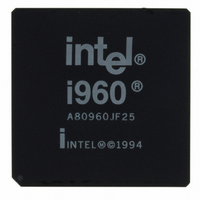
A80960JF3V25 Intel, A80960JF3V25 Datasheet - Page 18

A80960JF3V25
Manufacturer Part Number
A80960JF3V25
Description
IC MPU I960JF 3.3V 25MHZ 132-PGA
Manufacturer
Intel
Datasheet
1.NG80960JC66.pdf
(86 pages)
Specifications of A80960JF3V25
Processor Type
i960
Features
JF suffix, 32-Bit, 4K Cache
Speed
25MHz
Voltage
3.3V
Mounting Type
Surface Mount
Package / Case
132-PGA
Lead Free Status / RoHS Status
Lead free / RoHS Compliant
Other names
819540
Available stocks
Company
Part Number
Manufacturer
Quantity
Price
Company:
Part Number:
A80960JF3V25
Manufacturer:
Intel
Quantity:
135
80960JA/JF/JD/JS/JC/JT 3.3 V Embedded 32-Bit Microprocessor
18
Table 8.
Pin Description—External Bus Signals (Sheet 1 of 4)
AD[31:0]
NAME
A[3:2]
ALE#
ADS#
ALE
TYPE
R(X)
P(Q)
R(X)
P(Q)
S(L)
H(Z)
R(0)
H(Z)
P(0)
R(1)
H(Z)
P(1)
R(1)
H(Z)
P(1)
H(Z)
I/O
O
O
O
O
ADDRESS / DATA BUS carries 32-bit physical addresses and 8-, 16- or 32-bit data
to and from memory. During an address (
address (bits 0-1 indicate SIZE; see below). During a data (T
data is present on one or more contiguous bytes, comprising AD[31:24], AD[23:16],
AD[15:8] and AD[7:0]. During write operations, unused pins are driven to
determinate values.
SIZE, which comprises bits 0-1 of the AD lines during a
number of data transfers during the bus transaction.
AD1
0
0
1
1
When the processor enters Halt mode, if the previous bus operation was a:
Typically, AD[1:0] reflect the SIZE information of the last bus transaction (either
instruction fetch or load/store) that was executed before entering Halt mode.
ADDRESS LATCH ENABLE indicates the transfer of a physical address. ALE is
asserted during a
active HIGH and floats to a high impedance state during a hold cycle (T
ADDRESS LATCH ENABLE indicates the transfer of a physical address. ALE# is
the inverted version of ALE. This signal gives the 80960Jx a high degree of
compatibility with existing 80960Kx systems.
ADDRESS STROBE indicates a valid address and the start of a new bus access.
The processor asserts ADS# for the entire
typically samples ADS# at the end of the cycle.
ADDRESS[3:2] comprise a partial demultiplexed address bus.
32-bit memory accesses: the processor asserts address bits A[3:2] during
partial word address increments with each assertion of RDYRCV# during a burst.
16-bit memory accesses: the processor asserts address bits A[3:1] during
driven on the BE1# pin. The partial short word address increments with each
assertion of RDYRCV# during a burst.
8-bit memory accesses: the processor asserts address bits A[3:0] during
A[1:0] driven on BE[1:0]#. The partial byte address increments with each assertion of
RDYRCV# during a burst.
• write — AD[31:2] are driven with the last data value on the AD bus.
• read — AD[31:4] are driven with the last address value on the AD bus; AD[3:2]
are driven with the value of A[3:2] from the last data cycle.
AD0
0
1
0
1
T
a
cycle and deasserted before the beginning of the T
Bus Transfers
1 Transfer
2 Transfers
3 Transfers
4 Transfers
DESCRIPTION
T
a
T
) cycle, bits 31:2 contain a physical word
a
cycle. External bus control logic
T
a
cycle, specifies the
d
) cycle, read or write
h
d
Datasheet
).
T
state. It is
T
a
T
a
, with
a
with A1
. The


