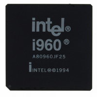
A80960JF3V25 Intel, A80960JF3V25 Datasheet - Page 9

A80960JF3V25
Manufacturer Part Number
A80960JF3V25
Description
IC MPU I960JF 3.3V 25MHZ 132-PGA
Manufacturer
Intel
Datasheet
1.NG80960JC66.pdf
(86 pages)
Specifications of A80960JF3V25
Processor Type
i960
Features
JF suffix, 32-Bit, 4K Cache
Speed
25MHz
Voltage
3.3V
Mounting Type
Surface Mount
Package / Case
132-PGA
Lead Free Status / RoHS Status
Lead free / RoHS Compliant
Other names
819540
Available stocks
Company
Part Number
Manufacturer
Quantity
Price
Company:
Part Number:
A80960JF3V25
Manufacturer:
Intel
Quantity:
135
80960JA/JF/JD/JS/JC/JT 3.3 V Embedded 32-Bit Microprocessor
2.0
80960Jx Overview
The 80960Jx processor offers high performance to cost-sensitive 32-bit embedded applications.
The 80960Jx is object code compatible with the 80960 core architecture and is capable of sustained
execution at the rate of one instruction per clock. This processor’s features include generous
instruction cache, data cache, and data RAM. It also boasts a fast interrupt mechanism and
dual-programmable timer units.
The 80960Jx processor’s clock multiplication operates the processor core at two or three times the
bus clock rate to improve execution performance without increasing the complexity of board
designs.
Memory subsystems for cost-sensitive embedded applications often impose substantial wait state
penalties. The 80960Jx integrates considerable storage resources on-chip to decouple CPU
execution from the external bus.
The 80960Jx rapidly allocates and de-allocates local register sets during context switches. The
processor must flush a register set to the stack only when it saves more than seven sets to its local
register cache.
A 32-bit multiplexed burst bus provides a high-speed interface to system memory and I/O. A full
complement of control signals simplifies the connection of the 80960Jx to external components.
The user programs physical and logical memory attributes through memory-mapped control
®
registers (MMRs), an extension not found on the i960
Kx, Sx or Cx processors. Physical and
logical configuration registers enable the processor to operate with all combinations of bus width
and data object alignment. The processor supports a homogeneous byte ordering model.
This processor integrates two important peripherals: a timer unit and an interrupt controller. These
and other hardware resources are programmed through memory-mapped control registers, an
extension to the familiar i960 processor architecture.
The timer unit (TU) offers two independent 32-bit timers for use as real-time system clocks and
general-purpose system timing. These operate in either single-shot or auto-reload mode and may
generate interrupts.
The interrupt controller unit (ICU) provides a flexible, low-latency means for requesting interrupts.
The ICU provides full programmability of up to 240 interrupt sources into 31 priority levels. The
ICU takes advantage of a cached priority table and optional routine caching to minimize interrupt
latency. Clock doubling on the 80960JD/JC processors reduces interrupt latency by 40% compared
to the 80960JA/JF, and clock tripling on the 80960JT reduces interrupt latency by 20% compared
to the 80960JD/JC. Local registers may be dedicated to high-priority interrupts to further reduce
latency. Acting independently from the core, the ICU compares the priorities of posted interrupts
with the current process priority, off-loading this task from the core. The ICU also supports the
integrated timer interrupts.
The 80960Jx features a Halt mode designed to support applications where low power consumption
is critical. The halt instruction shuts down instruction execution, resulting in a power savings of up
to 90 percent.
The 80960Jx’s testability features, including ONCE (On-Circuit Emulation) mode and Boundary
Scan (JTAG), provide a powerful environment for design debug and fault diagnosis.
Datasheet
9


