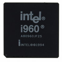
A80960JF3V25 Intel, A80960JF3V25 Datasheet - Page 45

A80960JF3V25
Manufacturer Part Number
A80960JF3V25
Description
IC MPU I960JF 3.3V 25MHZ 132-PGA
Manufacturer
Intel
Datasheet
1.NG80960JC66.pdf
(86 pages)
Specifications of A80960JF3V25
Processor Type
i960
Features
JF suffix, 32-Bit, 4K Cache
Speed
25MHz
Voltage
3.3V
Mounting Type
Surface Mount
Package / Case
132-PGA
Lead Free Status / RoHS Status
Lead free / RoHS Compliant
Other names
819540
Available stocks
Company
Part Number
Manufacturer
Quantity
Price
Company:
Part Number:
A80960JF3V25
Manufacturer:
Intel
Quantity:
135
4.7.1
Datasheet
Table 23. Note Definitions for Table 22, 80960Jx AC Characteristics
Figure 10. A.C. Test Load
A.C. Test Conditions and Derating Curves
The A.C. Specifications in
indicated in
Refer to the following sections for the specified derating curves:
NOTES:
10.Relative to falling edge of TCK.
11. Worst-case T
1. Not tested.
2. To ensure a 1:1 relationship between the amplitude of the input jitter and the internal clock, the jitter
3. Inactive ALE/ALE# refers to the falling edge of ALE and the rising edge of ALE#. For inactive ALE/ALE#
4. A float condition occurs when the output current becomes less than I
5. AD[31:0] are synchronous inputs. Setup and hold times must be met for proper processor operation. NMI#
6. RDYRCV# and HOLD are synchronous inputs. Setup and hold times must be met for proper processor
7. RESET# may be synchronous or asynchronous. Meeting setup and hold time guarantees recognition at a
8. ONCE# and STEST# must be stable at the rising edge of RESET# for proper operation.
9. Guaranteed by design. May not be 100% tested.
•
•
Output Pin
frequency spectrum should not have any power peaking between 500 KHz and 1/3 of the CLKIN
frequency.
timings, refer to Relative Output Timings in this table.
designed to be no longer than the valid delay.
and XINT[7:0]# may be synchronous or asynchronous. Meeting setup and hold time guarantees
recognition at a particular clock edge. For asynchronous operation, NMI# and XINT[7:0]# must be asserted
for a minimum of two CLKIN periods to ensure recognition.
operation.
particular clock edge.
output state. The Address/Data Bus pins encounter this condition between the last access of a read, and
the address cycle of a following write. 5 V signals take 3 ns longer to discharge than 3.3 V signals at 50 pF
loads.
Section 4.7.1.1, “Output Delay or Hold vs. Load Capacitance” on page 46
Section 4.7.1.2, “TLX vs. AD Bus Load Capacitance” on page 47
Figure
OV
condition occurs on I/O pins when pins transition from a floating high input to driving a low
10.
C
L
80960JA/JF/JD/JS/JC/JT 3.3 V Embedded 32-Bit Microprocessor
Section 4.7, “A.C. Specifications”
C
L
= 50 pF for all signals
are tested with the 50 pF load
OL
. Float delay is not tested, but is
45


