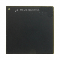
MC68EC060RC50 Freescale Semiconductor, MC68EC060RC50 Datasheet - Page 175

MC68EC060RC50
Manufacturer Part Number
MC68EC060RC50
Description
IC MPU 32BIT 50MHZ 206-PGA
Manufacturer
Freescale Semiconductor
Specifications of MC68EC060RC50
Processor Type
M680x0 32-Bit
Speed
50MHz
Voltage
3.3V
Mounting Type
Surface Mount
Package / Case
206-PGA
Family Name
M68000
Device Core
ColdFire
Device Core Size
32b
Frequency (max)
50MHz
Instruction Set Architecture
RISC
Supply Voltage 1 (typ)
3.3V
Operating Supply Voltage (max)
3.465V
Operating Supply Voltage (min)
3.135V
Operating Temp Range
0C to 110C
Operating Temperature Classification
Commercial
Mounting
Through Hole
Pin Count
206
Package Type
PGA
Lead Free Status / RoHS Status
Contains lead / RoHS non-compliant
Features
-
Lead Free Status / Rohs Status
Compliant
Available stocks
Company
Part Number
Manufacturer
Quantity
Price
Company:
Part Number:
MC68EC060RC50
Manufacturer:
NXP
Quantity:
1 746
- Current page: 175 of 416
- Download datasheet (2Mb)
Bus Operation
7.7.3 Byte, Word, and Long-Word Write Cycles
During a write transfer, the processor transfers data to a memory or peripheral device. The
level on the TCI signal is ignored by the processor during all write cycles. The bus controller
performs byte, word, and long-word write transfers for the following cases:
Figure 7-18 and Figure 7-19 illustrate a flowchart and functional timing diagram for byte,
word, and long-word write bus transfers.
7-20
• Accesses to a disabled cache
• Accesses to a memory page that is specified noncachable
• Accesses that are implicitly noncachable (locked read-modify-write accesses, access-
• Writes to writethrough pages
• Accesses that do not allocate in the data cache on a write miss (exception stacking)
• The first transfer of a line write is terminated with TBI, forcing completion of the line ac-
• Cache line pushes for lines containing a single dirty long word.
es to an alternate logical address space via the MOVES instruction, and table searches)
cess using three additional long-word write transfers
1) INCREMENT A3–A2
2) DRIVE SIZ1–SIZ0 TO LONG
3) ASSERT TS FOR ONE BCLK
4) ASSERT SAS IMMEDIATELY IF
1) NEGATE LOCK, LOCKE IF NECESSARY
1) NEGATE TIP OR START NEXT CYCLE
1) REGISTER DATA
ACKNOWLEDGE TERMINATION IGNORE
STATE CAPABILITY DISABLED. ELSE,
ASSERT SAS AFTER READ PRIMARY
IGNORE STATE COUNTER HAS EXPIRED
Figure 7-16. Burst-Inhibited Line Read Cycle Flowchart
PROCESSOR
4 LW DONE
M68060 USER’S MANUAL
CONTINUED FROM FIGURE 7-14
1) DECODE ADDRESS
2) PLACE DATA ON D31–D0
3) ASSERT TA FOR ONE BCLK
4) NEGATE CLA
1) THREE-STATE D31–D0
4 LW NOT DONE
SYSTEM
MOTOROLA
Related parts for MC68EC060RC50
Image
Part Number
Description
Manufacturer
Datasheet
Request
R
Part Number:
Description:
Manufacturer:
Freescale Semiconductor, Inc
Datasheet:
Part Number:
Description:
Manufacturer:
Freescale Semiconductor, Inc
Datasheet:
Part Number:
Description:
Manufacturer:
Freescale Semiconductor, Inc
Datasheet:
Part Number:
Description:
Manufacturer:
Freescale Semiconductor, Inc
Datasheet:
Part Number:
Description:
Manufacturer:
Freescale Semiconductor, Inc
Datasheet:
Part Number:
Description:
Manufacturer:
Freescale Semiconductor, Inc
Datasheet:
Part Number:
Description:
Manufacturer:
Freescale Semiconductor, Inc
Datasheet:
Part Number:
Description:
Manufacturer:
Freescale Semiconductor, Inc
Datasheet:
Part Number:
Description:
Manufacturer:
Freescale Semiconductor, Inc
Datasheet:
Part Number:
Description:
Manufacturer:
Freescale Semiconductor, Inc
Datasheet:
Part Number:
Description:
Manufacturer:
Freescale Semiconductor, Inc
Datasheet:
Part Number:
Description:
Manufacturer:
Freescale Semiconductor, Inc
Datasheet:
Part Number:
Description:
Manufacturer:
Freescale Semiconductor, Inc
Datasheet:
Part Number:
Description:
Manufacturer:
Freescale Semiconductor, Inc
Datasheet:
Part Number:
Description:
Manufacturer:
Freescale Semiconductor, Inc
Datasheet:


