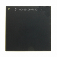
MC68EC060RC50 Freescale Semiconductor, MC68EC060RC50 Datasheet - Page 286

MC68EC060RC50
Manufacturer Part Number
MC68EC060RC50
Description
IC MPU 32BIT 50MHZ 206-PGA
Manufacturer
Freescale Semiconductor
Specifications of MC68EC060RC50
Processor Type
M680x0 32-Bit
Speed
50MHz
Voltage
3.3V
Mounting Type
Surface Mount
Package / Case
206-PGA
Family Name
M68000
Device Core
ColdFire
Device Core Size
32b
Frequency (max)
50MHz
Instruction Set Architecture
RISC
Supply Voltage 1 (typ)
3.3V
Operating Supply Voltage (max)
3.465V
Operating Supply Voltage (min)
3.135V
Operating Temp Range
0C to 110C
Operating Temperature Classification
Commercial
Mounting
Through Hole
Pin Count
206
Package Type
PGA
Lead Free Status / RoHS Status
Contains lead / RoHS non-compliant
Features
-
Lead Free Status / Rohs Status
Compliant
Available stocks
Company
Part Number
Manufacturer
Quantity
Price
Company:
Part Number:
MC68EC060RC50
Manufacturer:
NXP
Quantity:
1 746
- Current page: 286 of 416
- Download datasheet (2Mb)
9.2.1 Debug Command Interface
Figure 9-10 illustrates the debug command interface and Table 9-4 outlines the pins needed
by the debug command interface. The debug command interface consists of a five-bit shift
register and a five-bit parallel register, with each register operating independently. To acti-
vate the debug command interface, JTAG must be driven negated. This allows the debug
command interface to take over the regular JTAG interface and remap JTAG pin functions.
The resulting interface is fully synchronous to the CLK input.
The commands enter the debug command interface through the PTDI serial input signal into
the five-bit shift register. The shift register is controlled by the PSHIFT input. The PSHIFT
signal determines which rising CLK edge contains valid data on the PTDI input. When
asserted the PSHIFT input causes data from the PTDI input to be latched and causes inter-
nal data bits already in the shift register to be passed on to the next shift register bit. Serial
data eventually shifts out through the PTDO output. PTDO can be used as a status output
and can be used to verify that the shift register is operating properly. Do not assert both PAP-
PLY and PSHIFT on the same CLK edge as this is interpreted as a “no operation”.
MOTOROLA
TRST (PDISABLE)
TMS (PAPPLY)
TCK (PSHIFT)
TDO (PTDO)
Figure 9-10. Debug Command Interface Schematic
TDI (PTDI)
D31–D0
A31–A0
JTAG
CLK
Table 9-4. Debug Command Interface Pins
Pin Name
TRST
JTAG
TMS
TDO
TCK
CLK
TDI
MC68060 CHIP BOUNDARY
M68060 USER’S MANUAL
PDISABLE
PAPPLY
PSHIFT
PTDO
JTAG
CONTROLLER
Alias
PTDI
CLK
R
IEEE 1149.1 Test (JTAG) and Debug Pipe Control Modes
S
E
A
L
I
FLIP-FLOPS
TO ALL
P
A
R
A
E
L
L
L
BIT 0
BIT 4
Serial Command Data In
Debug Command Disable
Serial Command Data Out
JTAG or Debug Select
Clock
Serial Shift Enable
Command Apply Enable
COMMAND
COMMAND
WORD
VALID
5-BIT
Description
CONTROL LOGIC
OEP
9-25
Related parts for MC68EC060RC50
Image
Part Number
Description
Manufacturer
Datasheet
Request
R
Part Number:
Description:
Manufacturer:
Freescale Semiconductor, Inc
Datasheet:
Part Number:
Description:
Manufacturer:
Freescale Semiconductor, Inc
Datasheet:
Part Number:
Description:
Manufacturer:
Freescale Semiconductor, Inc
Datasheet:
Part Number:
Description:
Manufacturer:
Freescale Semiconductor, Inc
Datasheet:
Part Number:
Description:
Manufacturer:
Freescale Semiconductor, Inc
Datasheet:
Part Number:
Description:
Manufacturer:
Freescale Semiconductor, Inc
Datasheet:
Part Number:
Description:
Manufacturer:
Freescale Semiconductor, Inc
Datasheet:
Part Number:
Description:
Manufacturer:
Freescale Semiconductor, Inc
Datasheet:
Part Number:
Description:
Manufacturer:
Freescale Semiconductor, Inc
Datasheet:
Part Number:
Description:
Manufacturer:
Freescale Semiconductor, Inc
Datasheet:
Part Number:
Description:
Manufacturer:
Freescale Semiconductor, Inc
Datasheet:
Part Number:
Description:
Manufacturer:
Freescale Semiconductor, Inc
Datasheet:
Part Number:
Description:
Manufacturer:
Freescale Semiconductor, Inc
Datasheet:
Part Number:
Description:
Manufacturer:
Freescale Semiconductor, Inc
Datasheet:
Part Number:
Description:
Manufacturer:
Freescale Semiconductor, Inc
Datasheet:


