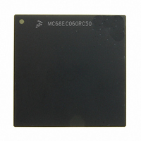
MC68EC060RC50 Freescale Semiconductor, MC68EC060RC50 Datasheet - Page 34

MC68EC060RC50
Manufacturer Part Number
MC68EC060RC50
Description
IC MPU 32BIT 50MHZ 206-PGA
Manufacturer
Freescale Semiconductor
Specifications of MC68EC060RC50
Processor Type
M680x0 32-Bit
Speed
50MHz
Voltage
3.3V
Mounting Type
Surface Mount
Package / Case
206-PGA
Family Name
M68000
Device Core
ColdFire
Device Core Size
32b
Frequency (max)
50MHz
Instruction Set Architecture
RISC
Supply Voltage 1 (typ)
3.3V
Operating Supply Voltage (max)
3.465V
Operating Supply Voltage (min)
3.135V
Operating Temp Range
0C to 110C
Operating Temperature Classification
Commercial
Mounting
Through Hole
Pin Count
206
Package Type
PGA
Lead Free Status / RoHS Status
Contains lead / RoHS non-compliant
Features
-
Lead Free Status / Rohs Status
Compliant
Available stocks
Company
Part Number
Manufacturer
Quantity
Price
Company:
Part Number:
MC68EC060RC50
Manufacturer:
NXP
Quantity:
1 746
- Current page: 34 of 416
- Download datasheet (2Mb)
Introduction
cute concurrently while the processor is performing an external access for a previous
instruction.
Each MC68060 cache is 8 Kbytes, accessed by physical addresses. The data cache can be
configured as write-through or deferred copyback on a page basis. This choice allows for
optimizing the system design for high performance if deferred copyback is used.
Cachability of data in each memory page is controlled by two bits in the page descriptor.
Cachable pages can be either write-through or copyback, with no write-allocate for misses
to write-through pages.
The MC68060 implements a four-entry store buffer that maximizes system performance by
decoupling the integer pipeline from the external system bus. When needed, the store buffer
allows the pipeline to generate writes every clock cycle until full, even if the system bus runs
at a slower speed than the processor.
1.4.2.6.1 Cache Organization. The instruction and data caches are each organized as
four-way set associative, with 16-byte lines. Each line of data has associated with it an
address tag and state information that shows the line’s validity. In the data cache, the state
information indicates whether the line is invalid, valid, or dirty.
1.4.2.6.2 Cache Coherency. The MC68060 has the ability to watch or snoop the external
bus during accesses by other bus masters, maintaining coherency between the MC68060's
caches and external memory systems. External bus cycles can be flagged on the bus as
snoopable or nonsnoopable. When an external cycle is marked as snoopable, the bus
snooper checks the caches and invalidates the matching data. Although the integer execu-
tion units and the bus snooper circuit have access to the on-chip caches, the snooper has
priority over the execution units.
1.4.3 Bus Controller
The bus is implemented as a nonmultiplexed, fully synchronous protocol that is clocked off
the rising edge of the input clock. The bus controller operates concurrently with all other
functional units of the MC68060 to maximize system throughput. The timing of the bus is
fully configurable to match external memory requirements.
1.5 PROCESSING STATES
The processor is always in one of three states: normal processing, exception processing, or
halted. It is in the normal processing state when executing instructions, fetching instructions
and operands, and storing instruction results.
Exception processing is the transition from program processing to system, interrupt, and
exception handling. Exception processing includes fetching the exception vector, stacking
operations, and refilling the instruction pipe caused after an exception. The processor enters
exception processing when an exceptional internal condition arises such as tracing an
instruction, an instruction results in a trap, or executing specific instructions. External condi-
tions, such as interrupts and access errors, also cause exceptions. Exception processing
ends when the first instruction of the exception handler begins to execute.
1-10
M68060 USER’S MANUAL
MOTOROLA
Related parts for MC68EC060RC50
Image
Part Number
Description
Manufacturer
Datasheet
Request
R
Part Number:
Description:
Manufacturer:
Freescale Semiconductor, Inc
Datasheet:
Part Number:
Description:
Manufacturer:
Freescale Semiconductor, Inc
Datasheet:
Part Number:
Description:
Manufacturer:
Freescale Semiconductor, Inc
Datasheet:
Part Number:
Description:
Manufacturer:
Freescale Semiconductor, Inc
Datasheet:
Part Number:
Description:
Manufacturer:
Freescale Semiconductor, Inc
Datasheet:
Part Number:
Description:
Manufacturer:
Freescale Semiconductor, Inc
Datasheet:
Part Number:
Description:
Manufacturer:
Freescale Semiconductor, Inc
Datasheet:
Part Number:
Description:
Manufacturer:
Freescale Semiconductor, Inc
Datasheet:
Part Number:
Description:
Manufacturer:
Freescale Semiconductor, Inc
Datasheet:
Part Number:
Description:
Manufacturer:
Freescale Semiconductor, Inc
Datasheet:
Part Number:
Description:
Manufacturer:
Freescale Semiconductor, Inc
Datasheet:
Part Number:
Description:
Manufacturer:
Freescale Semiconductor, Inc
Datasheet:
Part Number:
Description:
Manufacturer:
Freescale Semiconductor, Inc
Datasheet:
Part Number:
Description:
Manufacturer:
Freescale Semiconductor, Inc
Datasheet:
Part Number:
Description:
Manufacturer:
Freescale Semiconductor, Inc
Datasheet:


