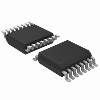
ADT7475ARQZ ON Semiconductor, ADT7475ARQZ Datasheet - Page 11

ADT7475ARQZ
Manufacturer Part Number
ADT7475ARQZ
Description
IC REMOTE THERMAL CTRLR 16-QSOP
Manufacturer
ON Semiconductor
Series
dBCool®r
Datasheet
1.ADT7475ARQZ.pdf
(58 pages)
Specifications of ADT7475ARQZ
Function
Fan Control, Temp Monitor
Topology
ADC, Comparator, Fan Speed Counter, Multiplexer, Register Bank
Sensor Type
External & Internal
Sensing Temperature
-40°C ~ 125°C, External Sensor
Output Type
SMBus™
Output Alarm
No
Output Fan
Yes
Voltage - Supply
3 V ~ 3.6 V
Operating Temperature
-40°C ~ 125°C
Mounting Type
Surface Mount
Package / Case
16-QSOP
Full Temp Accuracy
+/- 0.5 C
Digital Output - Bus Interface
Serial (3-Wire, 4-Wire)
Maximum Operating Temperature
+ 125 C
Minimum Operating Temperature
- 40 C
Lead Free Status / RoHS Status
Lead free / RoHS Compliant
Available stocks
Company
Part Number
Manufacturer
Quantity
Price
Part Number:
ADT7475ARQZ
Manufacturer:
ADI/亚德诺
Quantity:
20 000
Company:
Part Number:
ADT7475ARQZ-REEL7
Manufacturer:
SANYO
Quantity:
2 970
Part Number:
ADT7475ARQZ-REEL7
Manufacturer:
ADI/亚德诺
Quantity:
20 000
Part Number:
ADT7475ARQZ-RL7
Manufacturer:
ON/安森美
Quantity:
20 000
connected to a common SMBALERT line connected to the
master. If a device’s SMBALERT line goes low, the
following events occur:
SMBus Timeout
there is no SMBus activity for 35 ms, the ADT7475 assumes
that the bus is locked and releases the bus. This prevents the
device from locking or holding the SMBus expecting data.
Some SMBus controllers cannot handle the SMBus timeout
feature, so it can be disabled.
Configuration Register 1 (0x40)
Bit 6 TODIS = 0; SMBus timeout enabled (default).
Bit 6 TODIS = 1; SMBus timeout disabled.
Virus Protection
critical ADT7475 register settings, the lock bit can be set.
Setting Bit 1 of Configuration Register 1 (0x40) sets the lock
bit and locks critical registers. In this mode, certain registers
can no longer be written to until the ADT7475 is powered
down and powered up again. For more information on which
registers are locked, see the Register Tables section.
Voltage Measurement Input
channel. It can also measure its own supply voltage, V
Pin 14 can measure V
measurement is carried out through the V
V
in computer systems.
Analog−to−Digital Converter
successive approximation, analog−to−digital converter.
This has a resolution of 10 bits. The basic input range is 0 V
to 2.25 V, but the input has built−in attenuators to allow
measurement of V
CCP
The ADT7475 includes an SMBus timeout feature. If
To prevent rogue programs or viruses from accessing
The ADT7475 has one external voltage measurement
All analog inputs are multiplexed into the on−chip,
1. SMBALERT is pulled low.
2. The master initiates a read operation and sends the
3. The device whose SMBALERT output is low
4. If more than one device’s SMBALERT output is
5. Once the ADT7475 has responded to the alert
input can be used to monitor a chipset supply voltage
alert response address (ARA = 0001 100). This
general call address must not be used as a specific
device address.
responds to the alert response address, and the
master reads its device address. The address of the
device is now known and can be interrogated in
the usual way.
low, the one with the lowest device address has
priority in accordance with normal SMBus
arbitration.
response address, the master must read the status
registers, and the SMBALERT is cleared only if
the error condition has gone away.
CCP
without any external components. To
CCP
. The V
CC
CC
supply voltage
pin (Pin 3). The
http://onsemi.com
CC
.
11
allow for the tolerance of the supply voltage, the ADC
produces an output of 3/4 full scale (decimal 768 or 300 hex)
for the nominal input voltage and so has adequate headroom
to deal with overvoltages.
Input Circuitry
in Figure 19. The input circuit consists of an input protection
diode, an attenuator, and a capacitor to form a first−order,
low−pass filter that gives the input immunity to high
frequency noise.
Voltage Measurement Registers
Register 0x21, V
Register 0x22, V
V
and low limit register. Exceeding the programmed high or
low limit causes the appropriate status bit to be set.
Exceeding either limit can also generate SMBALERT
interrupts.
Register 0x46, V
Register 0x47, V
output codes of the 10−bit ADC.
voltage input in 711 ms and averages 16 conversions to
reduce noise; a measurement takes nominally 11.38 ms.
Extended Resolution Registers
using the extended resolution registers (0x76 and 0x77).
Whenever the extended resolution registers are read, the
corresponding data in the voltage measurement registers is
locked until their data is read. That is, if extended resolution
is required, then the extended resolution register must be
read first, immediately followed by the appropriate voltage
measurement register.
Additional ADC Functions for Voltage Measurements
ADT7475 to offer the system designer increased flexibility.
Turn−Off Averaging
16 readings have been made internally, and the
results averaged, before being placed into the value register.
For instances where faster conversions are needed, setting
Bit 4 of Configuration Register 2 (0x73) turns averaging off.
CCP
The internal structure for the V
Associated with the V
Table 2 shows the input ranges of the analog inputs and
When the ADC is running, it samples and converts a
Voltage measurements can be made with higher accuracy
A number of other functions are available on the
For each voltage measurement read from a value register,
Limit Registers
Figure 19. Structure of Analog Inputs
V
CCP
CCP
CC
CCP
CCP
Reading = 0x00 default
Reading = 0x00 default
Low Limit = 0x00 default
High Limit = 0xFF default
17.5kW
CCP
52.5kW
measurement channel is a high
CCP
analog input is shown
35pF


