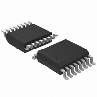
ADT7475ARQZ ON Semiconductor, ADT7475ARQZ Datasheet - Page 26

ADT7475ARQZ
Manufacturer Part Number
ADT7475ARQZ
Description
IC REMOTE THERMAL CTRLR 16-QSOP
Manufacturer
ON Semiconductor
Series
dBCool®r
Datasheet
1.ADT7475ARQZ.pdf
(58 pages)
Specifications of ADT7475ARQZ
Function
Fan Control, Temp Monitor
Topology
ADC, Comparator, Fan Speed Counter, Multiplexer, Register Bank
Sensor Type
External & Internal
Sensing Temperature
-40°C ~ 125°C, External Sensor
Output Type
SMBus™
Output Alarm
No
Output Fan
Yes
Voltage - Supply
3 V ~ 3.6 V
Operating Temperature
-40°C ~ 125°C
Mounting Type
Surface Mount
Package / Case
16-QSOP
Full Temp Accuracy
+/- 0.5 C
Digital Output - Bus Interface
Serial (3-Wire, 4-Wire)
Maximum Operating Temperature
+ 125 C
Minimum Operating Temperature
- 40 C
Lead Free Status / RoHS Status
Lead free / RoHS Compliant
Available stocks
Company
Part Number
Manufacturer
Quantity
Price
Part Number:
ADT7475ARQZ
Manufacturer:
ADI/亚德诺
Quantity:
20 000
Company:
Part Number:
ADT7475ARQZ-REEL7
Manufacturer:
SANYO
Quantity:
2 970
Part Number:
ADT7475ARQZ-REEL7
Manufacturer:
ADI/亚德诺
Quantity:
20 000
Part Number:
ADT7475ARQZ-RL7
Manufacturer:
ON/安森美
Quantity:
20 000
PWM Configuration Registers (0x5C to 0x5E)
Bits [7:5] BHVR
manually updated by writing to Register 0x30 to Register
0x32 (PWMx current duty cycle registers).
Programming the PWM Current Duty Cycle Registers
that allow the PWM duty cycle for each output to be set
anywhere from 0% to 100% in steps of 0.39%.
given by:
Example 1: For a PWM duty cycle of 50%,
Example 2: For a PWM duty cycle of 33%,
PWM Current Duty Cycle Registers
Register 0x30, PWM1 Current Duty Cycle = 0x00
(0% default)
Register 0x31, PWM2 Current Duty Cycle = 0x00
(0% default)
Register 0x32, PWM3 Current Duty Cycle = 0x00
(0% default)
user can keep track of the current duty cycle on each PWM
output, even when the fans are running in automatic fan
speed control mode or acoustic enhancement mode. See the
Programming the Automatic Fan Speed Control Loop
section for details.
Operating from 3.3 V Standby
from a 3.3 V STBY supply. In computers that support S3 and
S5 states, the core voltage of the processor is lowered in
these states. When monitoring THERM, the THERM timer
should be disabled during these states.
Standby Mode
the STBY supply. In computers that support S3 and S5 states,
the core voltage of the processor is lowered in these states.
When monitoring THERM, the THERM timer should be
disabled during these states.
the following occurs:
limit, everything is re−enabled and the system resumes
normal operation.
Once under manual control, each PWM output can be
The PWM current duty cycle registers are 8−bit registers
The value to be programmed into the PWM
By reading the PWMx current duty cycle registers, the
The ADT7475 has been specifically designed to operate
The ADT7475 has been specifically designed to respond to
When the V
Once the core voltage, V
111 = manual mode.
Value (decimal) = PWM
Value (decimal) = 50/0.39 = 128 (decimal)
Value = 128 (decimal) or 0x80 (hex)
Value (decimal) = 33/0.39 = 85 (decimal)
Value = 85 (decimal) or 0x54 (hex)
1. Status Bit 1 (V
2. SMBALERT is generated, if enabled.
3. THERM monitoring is disabled. The THERM timer
should hold its value prior to the S3 or S5 state.
CCP
voltage drops below the V
CCP
) in Status Register 1 is set.
CCP
MIN
, goes above the V
/0.39
CCP
MIN
low limit,
register is
CCP
http://onsemi.com
low
26
XNOR Tree Test Mode
mode is useful for in−circuit test equipment at board−level
testing. By applying stimulus to the pins included in the
XNOR tree, it is possible to detect opens or shorts on the
system board.
tree test mode. The XNOR tree test is invoked by setting Bit 0
(XEN) of the XNOR tree test enable register (0x6F).
Power−On Default
input.
is not powered up), the ADT7475 assumes the functionality
of the default registers after the ADT7475 is addressed via
any valid SMBus transaction.
The ADT7475 includes an XNOR tree test mode. This
Figure 40 shows the signals that are exercised in the XNOR
When the ADT7475 is powered up, it polls the V
If V
Y
Y
AFTER THE FAIL−SAFE TIMEOUT
CCP
FAIL−SAFE TIMER ELAPSES
ADT7475 IS POWERED UP
START FAIL−SAFE TIMER
HAS THE ADT7475 BEEN
HAS THE ADT7475 BEEN
HAS THE ADT7475 BEEN
SMBus TRANSACTION?
SMBus TRANSACTION?
SMBus TRANSACTION?
ACCESSED BY A VALID
ACCESSED BY A VALID
ACCESSED BY A VALID
IS V
ADT7475 NORMALLY
stays below 0.75 V (the system CPU power rail
Figure 41. Power−On Flow Chart
CCP
STARTUP THE
Figure 40. XNOR Tree Test
ABOVE 0.75V?
TACH1
TACH2
TACH3
TACH4
PWM2
PWM3
N
Y
N
Y
N
N
PWM1/XTO
HAS THE ADT7475 BEEN
SMBus TRANSACTION?
ACCESSED BY A VALID
SWITCH OFF FANS
RUNS THE FANS
TO FULL SPEED
CHECK V
Y
CCP
N
CCP


