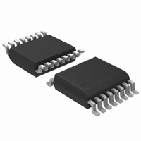
ADT7475ARQZ ON Semiconductor, ADT7475ARQZ Datasheet - Page 5

ADT7475ARQZ
Manufacturer Part Number
ADT7475ARQZ
Description
IC REMOTE THERMAL CTRLR 16-QSOP
Manufacturer
ON Semiconductor
Series
dBCool®r
Datasheet
1.ADT7475ARQZ.pdf
(58 pages)
Specifications of ADT7475ARQZ
Function
Fan Control, Temp Monitor
Topology
ADC, Comparator, Fan Speed Counter, Multiplexer, Register Bank
Sensor Type
External & Internal
Sensing Temperature
-40°C ~ 125°C, External Sensor
Output Type
SMBus™
Output Alarm
No
Output Fan
Yes
Voltage - Supply
3 V ~ 3.6 V
Operating Temperature
-40°C ~ 125°C
Mounting Type
Surface Mount
Package / Case
16-QSOP
Full Temp Accuracy
+/- 0.5 C
Digital Output - Bus Interface
Serial (3-Wire, 4-Wire)
Maximum Operating Temperature
+ 125 C
Minimum Operating Temperature
- 40 C
Lead Free Status / RoHS Status
Lead free / RoHS Compliant
Available stocks
Company
Part Number
Manufacturer
Quantity
Price
Part Number:
ADT7475ARQZ
Manufacturer:
ADI/亚德诺
Quantity:
20 000
Company:
Part Number:
ADT7475ARQZ-REEL7
Manufacturer:
SANYO
Quantity:
2 970
Part Number:
ADT7475ARQZ-REEL7
Manufacturer:
ADI/亚德诺
Quantity:
20 000
Part Number:
ADT7475ARQZ-RL7
Manufacturer:
ON/安森美
Quantity:
20 000
ELECTRICAL CHARACTERISTICS
DIGITAL INPUT LOGIC LEVELS (THERM) ADTL+
DIGITAL INPUT CURRENT
SERIAL BUS TIMING
1. All voltages are measured with respect to GND, unless otherwise specified. Typicals are at T
2. SMBus timing specifications are guaranteed by design and are not production tested.
Input High Voltage, V
Input Low Voltage, V
Input High Current, I
Input Low Current, I
Input Capacitance, C
Clock Frequency, f
Glitch Immunity, t
Bus Free Time, t
SCL Low Time, t
SCL High Time, t
SCL, SDA Rise Time, t
SCL, SDA Fall Time, t
Data Setup Time, t
Detect Clock Low Timeout, t
parametric norm. Logic inputs accept input high voltages of up to V
specifications are tested at logic levels of V
SDA
SCL
P
t
BUF
BUF
LOW
HIGH
SW
Parameter
S
SCLK
SU: DAT
IL
IH
IL
IH
IN
F
t
R
HD: STA
TIMEOUT
t
LOW
t
R
t
HD: DAT
T
A
= T
Figure 2. Serial Bus Timing Diagram
IL
MIN
= 0.8 V for a falling edge and V
V
V
See Note 2 and Figure 2
Can be optionally disabled
to T
IN
IN
t
HIGH
= V
= 0 V
MAX
http://onsemi.com
t
F
CC
t
SU: DAT
, V
CC
Conditions
= V
5
MIN
MAX
to V
, even when the device is operating down to V
MAX
IH
S
, unless otherwise noted. (Note 1)
= 2.0 V for a rising edge.
t
SU: STA
t
HD: STA
0.75 x V
Min
250
4.7
4.7
4.0
10
15
A
= 25°C and represent the most likely
CC
Typ
±1
±1
5
t
SU: STO
1000
Max
400
300
0.8
50
50
35
MIN
P
. Timing
Unit
kHz
mA
mA
ms
pF
ns
ms
ms
ms
ns
ms
ns
V
V


