DEMO9S08LC60 Freescale Semiconductor, DEMO9S08LC60 Datasheet - Page 186
DEMO9S08LC60
Manufacturer Part Number
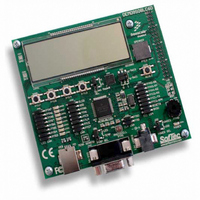
DEMO9S08LC60
Description
BOARD DEMO FOR 9S08LC60
Manufacturer
Freescale Semiconductor
Type
MCUr
Datasheets
1.DEMO9S08LC60.pdf
(360 pages)
2.DEMO9S08LC60.pdf
(32 pages)
3.DEMO9S08LC60.pdf
(2 pages)
Specifications of DEMO9S08LC60
Contents
Evaluation Board
Processor To Be Evaluated
MC9S08LC60
Interface Type
RS-232, USB
Silicon Manufacturer
Freescale
Core Architecture
HCS08
Core Sub-architecture
HCS08
Silicon Core Number
MC9S08
Silicon Family Name
S08LC
Rohs Compliant
Yes
For Use With/related Products
MC9S08LC60
Lead Free Status / RoHS Status
Lead free / RoHS Compliant


1
2
3
Chapter 10 Internal Clock Generator (S08ICGV4)
10.5.10 Clock Mode Requirements
A clock mode is requested by writing to CLKS1:CLKS0 and the actual clock mode is indicated by
CLKST1:CLKST0. Provided minimum conditions are met, the status shown in CLKST1:CLKST0 should
be the same as the requested mode in CLKS1:CLKS0.
CLKST, and ICGOUT. It also shows the conditions for CLKS = CLKST or the reason CLKS ≠ CLKST.
186
(CLKST)
CLKST will not update immediately after a write to CLKS. Several bus cycles are required before CLKST updates to the new
value.
The reference frequency has no effect on ICGOUT in SCM, but the reference frequency is still used in making the comparisons
that determine the DCOS bit
After initial LOCK; will be ICGDCLK/2R during initial locking process and while FLL is re-locking after the MFD bits are changed.
Actual
Mode
SCM
(XX)
FBE
FEE
(00)
(01)
(10)
(11)
FEI
Off
Desired
(CLKS)
Mode
SCM
(XX)
FBE
FBE
FEE
FEE
FBE
FEE
FEE
(10)
(00)
(01)
(10)
(11)
(01)
(11)
(10)
(11)
(11)
FEI
FEI
Off
If a crystal will be used before the next reset, then be sure to set REFS = 1
and CLKS = 1x on the first write to the ICGC1 register. Failure to do so will
result in “locking” REFS = 0 which will prevent the oscillator amplifier
from being enabled until the next reset occurs.
Range
X
X
X
X
X
X
X
X
0
0
0
1
MC9S08LC60 Series Data Sheet: Technical Data, Rev. 4
(f
f
f
f
f
ICGIRCLK
ICGIRCLK
ICGIRCLK
Frequency
Reference
f
f
ICGIRCLK
REFERENCE
ICGIRCLK
ICGIRCLK
f
f
ICGERCLK
ICGERCLK
0
0
0
0
Table 10-9. ICG State Table
/7
/7
/7
/7
/7
/7
(1)
(1)
(1)
2
)
128/f
Comparison
Cycle Time
2/f
8/f
8/f
8/f
8/f
8/f
8/f
NOTE
ICGERCLK
ICGIRCLK
ICGIRCLK
ICGIRCLK
ICGIRCLK
ICGIRCLK
ICGIRCLK
ICGERCLK
—
—
—
—
Table 10-9
ICGDCLK/R
ICGERCLK/R
ICGERCLK/R
ICGDCLK/R
ICGDCLK/R
ICGDCLK/R
ICGDCLK/R
ICGDCLK/R
ICGDCLK/R
ICGDCLK/R
ICGOUT
shows the relationship between CLKS,
0
0
(2)
3
Conditions
CLKS = CLKST
ERCS = 1 and
ERCS = 1 and
Not switching
from FBE to
DCOS = 1
ERCS = 1
DCOS = 1
DCOS = 1
SCM
—
—
—
—
—
—
—
Freescale Semiconductor
1
for
DCOS = 0 or
LOCS = 1 &
DCOS = 0
ERCS = 0
ERCS = 0
ERCS = 0
ERCS = 0
ERCS = 1
CLKS1 ≠
Reason
CLKST
—
—
—
—
—
—
Related parts for DEMO9S08LC60
Image
Part Number
Description
Manufacturer
Datasheet
Request
R

Part Number:
Description:
Manufacturer:
Freescale Semiconductor, Inc
Datasheet:
Part Number:
Description:
Manufacturer:
Freescale Semiconductor, Inc
Datasheet:
Part Number:
Description:
Manufacturer:
Freescale Semiconductor, Inc
Datasheet:
Part Number:
Description:
Manufacturer:
Freescale Semiconductor, Inc
Datasheet:
Part Number:
Description:
Manufacturer:
Freescale Semiconductor, Inc
Datasheet:
Part Number:
Description:
Manufacturer:
Freescale Semiconductor, Inc
Datasheet:
Part Number:
Description:
Manufacturer:
Freescale Semiconductor, Inc
Datasheet:
Part Number:
Description:
Manufacturer:
Freescale Semiconductor, Inc
Datasheet:
Part Number:
Description:
Manufacturer:
Freescale Semiconductor, Inc
Datasheet:
Part Number:
Description:
Manufacturer:
Freescale Semiconductor, Inc
Datasheet:
Part Number:
Description:
Manufacturer:
Freescale Semiconductor, Inc
Datasheet:
Part Number:
Description:
Manufacturer:
Freescale Semiconductor, Inc
Datasheet:
Part Number:
Description:
Manufacturer:
Freescale Semiconductor, Inc
Datasheet:
Part Number:
Description:
Manufacturer:
Freescale Semiconductor, Inc
Datasheet:
Part Number:
Description:
Manufacturer:
Freescale Semiconductor, Inc
Datasheet: