DEMO9S08LC60 Freescale Semiconductor, DEMO9S08LC60 Datasheet - Page 58
DEMO9S08LC60
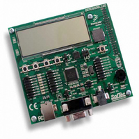
Manufacturer Part Number
DEMO9S08LC60
Description
BOARD DEMO FOR 9S08LC60
Manufacturer
Freescale Semiconductor
Type
MCUr
Datasheets
1.DEMO9S08LC60.pdf
(360 pages)
2.DEMO9S08LC60.pdf
(32 pages)
3.DEMO9S08LC60.pdf
(2 pages)
Specifications of DEMO9S08LC60
Contents
Evaluation Board
Processor To Be Evaluated
MC9S08LC60
Interface Type
RS-232, USB
Silicon Manufacturer
Freescale
Core Architecture
HCS08
Core Sub-architecture
HCS08
Silicon Core Number
MC9S08
Silicon Family Name
S08LC
Rohs Compliant
Yes
For Use With/related Products
MC9S08LC60
Lead Free Status / RoHS Status
Lead free / RoHS Compliant


Chapter 4 Memory
4.6.3
Bits 7 through 5 may be read or written at any time. Bits 4 through 0 always read 0 and cannot be written.
4.6.4
The FPROT register defines which FLASH sectors are protected against program and erase operations.
The FPROT register is also used to determine whether FLASH protection is disabled.
During the reset sequence, the FPROT register is loaded from the nonvolatile location NVPROT. To
change the protection that will be loaded during the reset sequence, the sector containing NVPROT must
be unprotected and erased, then NVPROT can be reprogrammed. With FPDIS set all FPROT bits are
writable, but with FPDIS clear the FPS bits are writable as long as the size of the protected region is being
increased. Any write to FPROT that attempts to decrease the size of the protected memory will be ignored.
Trying to alter data in any protected area will result in a protection violation error and the FPVIOL flag
will be set in the FSTAT register. Mass erase is not possible if any one of the sectors is protected.
In order to change the data flash block protection on a temporary basis, the FPROT register EPS bits can
be written to. To change the data flash block protection that will be loaded during the reset sequence, the
58
KEYACC
Reset
Field
5
W
R
FLASH Configuration Register (FCNFG)
FLASH Protection Register (FPROT and NVPROT)
Enable Writing of Access Key — This bit enables writing of the backdoor comparison key. For more detailed
information about the backdoor key mechanism, refer to
0 Writes to 0xFFB0–0xFFB7 are interpreted as the start of a FLASH programming or erase command.
1 Writes to NVBACKKEY (0xFFB0–0xFFB7) are interpreted as comparison key writes.
0
0
7
1
= Unimplemented or Reserved
The 0:1 bit pattern is the recommended value to be used since it requires two
bit changes before going to the unsecured state.
0
0
6
Figure 4-7. FLASH Configuration Register (FCNFG)
MC9S08LC60 Series Data Sheet: Technical Data, Rev. 4
SEC01:SEC00
0:1
Table 4-10. FCNFG Field Descriptions
0:0
1:0
1:1
KEYACC
1
0
5
Table 4-9. Security States
0
0
4
Description
Section 4.5,
3
0
0
Description
unsecured
secure
secure
secure
“Security.”
0
0
2
Freescale Semiconductor
0
0
1
0
0
0
Related parts for DEMO9S08LC60
Image
Part Number
Description
Manufacturer
Datasheet
Request
R

Part Number:
Description:
Manufacturer:
Freescale Semiconductor, Inc
Datasheet:
Part Number:
Description:
Manufacturer:
Freescale Semiconductor, Inc
Datasheet:
Part Number:
Description:
Manufacturer:
Freescale Semiconductor, Inc
Datasheet:
Part Number:
Description:
Manufacturer:
Freescale Semiconductor, Inc
Datasheet:
Part Number:
Description:
Manufacturer:
Freescale Semiconductor, Inc
Datasheet:
Part Number:
Description:
Manufacturer:
Freescale Semiconductor, Inc
Datasheet:
Part Number:
Description:
Manufacturer:
Freescale Semiconductor, Inc
Datasheet:
Part Number:
Description:
Manufacturer:
Freescale Semiconductor, Inc
Datasheet:
Part Number:
Description:
Manufacturer:
Freescale Semiconductor, Inc
Datasheet:
Part Number:
Description:
Manufacturer:
Freescale Semiconductor, Inc
Datasheet:
Part Number:
Description:
Manufacturer:
Freescale Semiconductor, Inc
Datasheet:
Part Number:
Description:
Manufacturer:
Freescale Semiconductor, Inc
Datasheet:
Part Number:
Description:
Manufacturer:
Freescale Semiconductor, Inc
Datasheet:
Part Number:
Description:
Manufacturer:
Freescale Semiconductor, Inc
Datasheet:
Part Number:
Description:
Manufacturer:
Freescale Semiconductor, Inc
Datasheet: