DEMO9S08LC60 Freescale Semiconductor, DEMO9S08LC60 Datasheet - Page 48
DEMO9S08LC60
Manufacturer Part Number
DEMO9S08LC60
Description
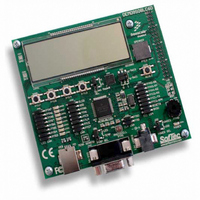
BOARD DEMO FOR 9S08LC60
Manufacturer
Freescale Semiconductor
Type
MCUr
Datasheets
1.DEMO9S08LC60.pdf
(360 pages)
2.DEMO9S08LC60.pdf
(32 pages)
3.DEMO9S08LC60.pdf
(2 pages)
Specifications of DEMO9S08LC60
Contents
Evaluation Board
Processor To Be Evaluated
MC9S08LC60
Interface Type
RS-232, USB
Silicon Manufacturer
Freescale
Core Architecture
HCS08
Core Sub-architecture
HCS08
Silicon Core Number
MC9S08
Silicon Family Name
S08LC
Rohs Compliant
Yes
For Use With/related Products
MC9S08LC60
Lead Free Status / RoHS Status
Lead free / RoHS Compliant


Chapter 4 Memory
The RAM retains data when the MCU is in low-power wait, stop2, or stop3 mode. At power-on or after
wakeup from stop1, the contents of RAM are uninitialized. RAM data is unaffected by any reset provided
that the supply voltage does not drop below the minimum value for RAM retention.
For compatibility with older M68HC05 MCUs, the HCS08 resets the stack pointer to 0x00FF. In the
MC9S08LC60 Series, it is usually best to re-initialize the stack pointer to the top of the RAM so the direct
page RAM can be used for frequently accessed RAM variables and bit-addressable program variables.
Include the following 2-instruction sequence in your reset initialization routine (where RamLast is equated
to the highest address of the RAM in the Freescale-provided equate file).
When security is enabled, the RAM is considered a secure memory resource and is not accessible through
BDM or through code executing from non-secure memory. See
description of the security feature.
4.4
The FLASH memory is intended primarily for program storage. In-circuit programming allows the
operating program to be loaded into the FLASH memory after final assembly of the application product.
It is possible to program the entire array through the single-wire background debug interface. Because no
special voltages are needed for FLASH erase and programming operations, in-application programming
is also possible through other software-controlled communication paths. For a more detailed discussion of
in-circuit and in-application programming, refer to the HCS08 Family Reference Manual, Volume I,
Freescale Semiconductor document order number HCS08RMv1/D.
Because the MC9S08LC60 Series contains two FLASH arrays, program and erase operations can be
conducted on one array while executing code from the other. The security and protection features treat the
two arrays as a single memory entity. Programming and erasing of each FLASH array is conducted
through the same command interface detailed in the following sections.
It is not possible to page erase or program both arrays at the same time. The mass erase command will
erase both arrays, and the blank check command will check both arrays.
48
FLASH
LDHX
TXS
#RamLast+1
MC9S08LC60 Series Data Sheet: Technical Data, Rev. 4
;point one past RAM
;SP<-(H:X-1)
Section 4.5,
“Security”
Freescale Semiconductor
for a detailed
Related parts for DEMO9S08LC60
Image
Part Number
Description
Manufacturer
Datasheet
Request
R

Part Number:
Description:
Manufacturer:
Freescale Semiconductor, Inc
Datasheet:
Part Number:
Description:
Manufacturer:
Freescale Semiconductor, Inc
Datasheet:
Part Number:
Description:
Manufacturer:
Freescale Semiconductor, Inc
Datasheet:
Part Number:
Description:
Manufacturer:
Freescale Semiconductor, Inc
Datasheet:
Part Number:
Description:
Manufacturer:
Freescale Semiconductor, Inc
Datasheet:
Part Number:
Description:
Manufacturer:
Freescale Semiconductor, Inc
Datasheet:
Part Number:
Description:
Manufacturer:
Freescale Semiconductor, Inc
Datasheet:
Part Number:
Description:
Manufacturer:
Freescale Semiconductor, Inc
Datasheet:
Part Number:
Description:
Manufacturer:
Freescale Semiconductor, Inc
Datasheet:
Part Number:
Description:
Manufacturer:
Freescale Semiconductor, Inc
Datasheet:
Part Number:
Description:
Manufacturer:
Freescale Semiconductor, Inc
Datasheet:
Part Number:
Description:
Manufacturer:
Freescale Semiconductor, Inc
Datasheet:
Part Number:
Description:
Manufacturer:
Freescale Semiconductor, Inc
Datasheet:
Part Number:
Description:
Manufacturer:
Freescale Semiconductor, Inc
Datasheet:
Part Number:
Description:
Manufacturer:
Freescale Semiconductor, Inc
Datasheet: