DEMO9S08LC60 Freescale Semiconductor, DEMO9S08LC60 Datasheet - Page 289
DEMO9S08LC60
Manufacturer Part Number
DEMO9S08LC60
Description
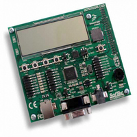
BOARD DEMO FOR 9S08LC60
Manufacturer
Freescale Semiconductor
Type
MCUr
Datasheets
1.DEMO9S08LC60.pdf
(360 pages)
2.DEMO9S08LC60.pdf
(32 pages)
3.DEMO9S08LC60.pdf
(2 pages)
Specifications of DEMO9S08LC60
Contents
Evaluation Board
Processor To Be Evaluated
MC9S08LC60
Interface Type
RS-232, USB
Silicon Manufacturer
Freescale
Core Architecture
HCS08
Core Sub-architecture
HCS08
Silicon Core Number
MC9S08
Silicon Family Name
S08LC
Rohs Compliant
Yes
For Use With/related Products
MC9S08LC60
Lead Free Status / RoHS Status
Lead free / RoHS Compliant


In cases where separate power supplies are used for analog and digital power, the ground connection
between these supplies must be at the V
supplies if possible. The V
15.6.1.2
In addition to the analog supplies, the ADC module has connections for two reference voltage inputs. The
high reference is V
reference is V
When available on a separate pin, V
driven by an external source that is between the minimum V
must never exceed V
voltage potential as V
immunity and bypass capacitors placed as near as possible to the package.
AC current in the form of current spikes required to supply charge to the capacitor array at each successive
approximation step is drawn through the V
current demand is a 0.1 μF capacitor with good high frequency characteristics. This capacitor is connected
between V
path is not recommended because the current will cause a voltage drop which could result in conversion
errors. Inductance in this path must be minimum (parasitic only).
15.6.1.3
The external analog inputs are typically shared with digital I/O pins on MCU devices. The pin I/O control
is disabled by setting the appropriate control bit in one of the pin control registers. Conversions can be
performed on inputs without the associated pin control register bit set. It is recommended that the pin
control register bit always be set when using a pin as an analog input. This avoids problems with contention
because the output buffer will be in its high impedance state and the pullup is disabled. Also, the input
buffer draws DC current when its input is not at either V
all pins used as analog inputs should be done to achieve lowest operating current.
Empirical data shows that capacitors on the analog inputs improve performance in the presence of noise
or when the source impedance is high. Use of 0.01 μF capacitors with good high-frequency characteristics
is sufficient. These capacitors are not necessary in all cases, but when used they must be placed as near as
possible to the package pins and be referenced to V
For proper conversion, the input voltage must fall between V
exceeds V
(full scale 10-bit representation) or $FF (full scale 8-bit representation). If the input is equal to or less than
V
linear conversions. There will be a brief current associated with V
charging. The input is sampled for 3.5 cycles of the ADCK source when ADLSMP is low, or 23.5 cycles
when ADLSMP is high.
For minimal loss of accuracy due to current injection, pins adjacent to the analog input pins should not be
transitioning during conversions.
Freescale Semiconductor
REFL
, the converter circuit converts it to $000. Input voltages between V
REFH
REFH
Analog Reference Pins
Analog Input Pins
REFL
, the converter circuit converts the signal to $FFF (full scale 12-bit representation), $3FF
and V
, which may be shared on the same pin as V
REFH
DDAD
SSAD
REFL
, which may be shared on the same pin as V
). When available on a separate pin, V
SSAD
. Both V
and must be placed as near as possible to the package pins. Resistance in the
MC9S08LC60 Series Data Sheet: Technical Data, Rev. 4
pin makes a good single point ground location.
REFH
REFH
SSAD
and V
may be connected to the same potential as V
REFH
pin. This should be the only ground connection between these
REFL
and V
SSA
must be routed carefully for maximum noise
REFL
.
DD
loop. The best external component to meet this
or V
DDAD
REFH
Chapter 15 Analog-to-Digital Converter (S08ADC12V1)
SSAD
SS
REFL
. Setting the pin control register bits for
REFL
spec and the V
and V
DDAD
on some devices.
must be connected to the same
when the sampling capacitor is
REFH
REFL
on some devices. The low
. If the input is equal to or
and V
DDAD
REFL
DDAD
potential (V
are straight-line
, or may be
REFH
289
Related parts for DEMO9S08LC60
Image
Part Number
Description
Manufacturer
Datasheet
Request
R

Part Number:
Description:
Manufacturer:
Freescale Semiconductor, Inc
Datasheet:
Part Number:
Description:
Manufacturer:
Freescale Semiconductor, Inc
Datasheet:
Part Number:
Description:
Manufacturer:
Freescale Semiconductor, Inc
Datasheet:
Part Number:
Description:
Manufacturer:
Freescale Semiconductor, Inc
Datasheet:
Part Number:
Description:
Manufacturer:
Freescale Semiconductor, Inc
Datasheet:
Part Number:
Description:
Manufacturer:
Freescale Semiconductor, Inc
Datasheet:
Part Number:
Description:
Manufacturer:
Freescale Semiconductor, Inc
Datasheet:
Part Number:
Description:
Manufacturer:
Freescale Semiconductor, Inc
Datasheet:
Part Number:
Description:
Manufacturer:
Freescale Semiconductor, Inc
Datasheet:
Part Number:
Description:
Manufacturer:
Freescale Semiconductor, Inc
Datasheet:
Part Number:
Description:
Manufacturer:
Freescale Semiconductor, Inc
Datasheet:
Part Number:
Description:
Manufacturer:
Freescale Semiconductor, Inc
Datasheet:
Part Number:
Description:
Manufacturer:
Freescale Semiconductor, Inc
Datasheet:
Part Number:
Description:
Manufacturer:
Freescale Semiconductor, Inc
Datasheet:
Part Number:
Description:
Manufacturer:
Freescale Semiconductor, Inc
Datasheet: