M68EVB908GB60E Freescale Semiconductor, M68EVB908GB60E Datasheet - Page 181
M68EVB908GB60E
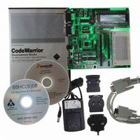
Manufacturer Part Number
M68EVB908GB60E
Description
BOARD EVAL FOR MC9S08GB60
Manufacturer
Freescale Semiconductor
Type
MCUr
Datasheet
1.M68EVB908GB60E.pdf
(290 pages)
Specifications of M68EVB908GB60E
Contents
Module and Misc Hardware
Processor To Be Evaluated
MC9S08GB
Data Bus Width
8 bit
Interface Type
RS-232
Silicon Manufacturer
Freescale
Core Architecture
HCS08
Core Sub-architecture
HCS08
Silicon Core Number
MC9S08
Silicon Family Name
S08GB
Kit Contents
GB60 Evaluation Kit
Rohs Compliant
Yes
For Use With/related Products
MC9S08GB60
Lead Free Status / RoHS Status
Lead free / RoHS Compliant


RE — Receiver Enable
RWU — Receiver Wakeup Control
SBK — Send Break
11.10.4 SCI x Status Register 1 (SCIxS1)
This register has eight read-only status flags. Writes have no effect. Special software sequences (that do
not involve writing to this register) are used to clear these status flags.
TDRE — Transmit Data Register Empty Flag
Freescale Semiconductor
When the SCI receiver is off, the RxD1 pin reverts to being a general-purpose port I/O pin.
This bit can be written to 1 to place the SCI receiver in a standby state where it waits for automatic
hardware detection of a selected wakeup condition. The wakeup condition is either an idle line between
messages (WAKE = 0, idle-line wakeup), or a logic 1 in the most significant data bit in a character
(WAKE = 1, address-mark wakeup). Application software sets RWU and (normally) a selected
hardware condition automatically clears RWU. Refer to
Operation,”
Writing a 1 and then a 0 to SBK queues a break character in the transmit data stream. Additional break
characters of 10 or 11 bit times of logic 0 are queued as long as SBK = 1. Depending on the timing of
the set and clear of SBK relative to the information currently being transmitted, a second break
character may be queued before software clears SBK. Refer to
Queued
TDRE is set out of reset and when a transmit data value transfers from the transmit data buffer to the
transmit shifter, leaving room for a new character in the buffer. To clear TDRE, read SCIxS1 with
TDRE = 1 and then write to the SCI data register (SCIxD).
1 = Receiver on.
0 = Receiver off.
1 = SCI receiver in standby waiting for wakeup condition.
0 = Normal SCI receiver operation.
1 = Queue break character(s) to be sent.
0 = Normal transmitter operation.
1 = Transmit data register (buffer) empty.
0 = Transmit data register (buffer) full.
Idle,”
for more details.
for more details.
Reset:
Read:
Write:
TDRE
Bit 7
1
Figure 11-9. SCI x Status Register 1 (SCIxS1)
= Unimplemented or Reserved
MC9S08GB/GT Data Sheet, Rev. 2.3
TC
6
1
RDRF
5
0
IDLE
4
0
Section 11.6.3, “Receiver Wakeup
OR
3
0
Section 11.5.2, “Send Break and
NF
2
0
SCI Registers and Control Bits
FE
1
0
Bit 0
PF
0
181
Related parts for M68EVB908GB60E
Image
Part Number
Description
Manufacturer
Datasheet
Request
R

Part Number:
Description:
Manufacturer:
Freescale Semiconductor, Inc
Datasheet:
Part Number:
Description:
Manufacturer:
Freescale Semiconductor, Inc
Datasheet:
Part Number:
Description:
Manufacturer:
Freescale Semiconductor, Inc
Datasheet:
Part Number:
Description:
Manufacturer:
Freescale Semiconductor, Inc
Datasheet:
Part Number:
Description:
Manufacturer:
Freescale Semiconductor, Inc
Datasheet:
Part Number:
Description:
Manufacturer:
Freescale Semiconductor, Inc
Datasheet:
Part Number:
Description:
Manufacturer:
Freescale Semiconductor, Inc
Datasheet:
Part Number:
Description:
Manufacturer:
Freescale Semiconductor, Inc
Datasheet:
Part Number:
Description:
Manufacturer:
Freescale Semiconductor, Inc
Datasheet:
Part Number:
Description:
Manufacturer:
Freescale Semiconductor, Inc
Datasheet:
Part Number:
Description:
Manufacturer:
Freescale Semiconductor, Inc
Datasheet:
Part Number:
Description:
Manufacturer:
Freescale Semiconductor, Inc
Datasheet:
Part Number:
Description:
Manufacturer:
Freescale Semiconductor, Inc
Datasheet:
Part Number:
Description:
Manufacturer:
Freescale Semiconductor, Inc
Datasheet:
Part Number:
Description:
Manufacturer:
Freescale Semiconductor, Inc
Datasheet: