M68EVB908GB60E Freescale Semiconductor, M68EVB908GB60E Datasheet - Page 29
M68EVB908GB60E
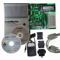
Manufacturer Part Number
M68EVB908GB60E
Description
BOARD EVAL FOR MC9S08GB60
Manufacturer
Freescale Semiconductor
Type
MCUr
Datasheet
1.M68EVB908GB60E.pdf
(290 pages)
Specifications of M68EVB908GB60E
Contents
Module and Misc Hardware
Processor To Be Evaluated
MC9S08GB
Data Bus Width
8 bit
Interface Type
RS-232
Silicon Manufacturer
Freescale
Core Architecture
HCS08
Core Sub-architecture
HCS08
Silicon Core Number
MC9S08
Silicon Family Name
S08GB
Kit Contents
GB60 Evaluation Kit
Rohs Compliant
Yes
For Use With/related Products
MC9S08GB60
Lead Free Status / RoHS Status
Lead free / RoHS Compliant


debug connector so a development system can directly reset the MCU system. If desired, a manual external
reset can be added by supplying a simple switch to ground (pull reset pin low to force a reset).
Whenever any reset is initiated (whether from an external signal or from an internal system), the reset pin
is driven low for approximately 34 cycles of f
cycles of f
timeout, the circuitry expects the reset pin sample to return a logic 1. If the pin is still low at this sample
point, the reset is assumed to be from an external source. The reset circuitry decodes the cause of reset and
records it by setting a corresponding bit in the system control reset status register (SRS).
Never connect any significant capacitance to the reset pin because that would interfere with the circuit and
sequence that detects the source of reset. If an external capacitance prevents the reset pin from rising to a
valid logic 1 before the reset sample point, all resets will appear to be external resets.
2.3.4
The background/mode select (BKGD/MS) shares its function with an I/O port pin. While in reset, the pin
functions as a mode select pin. Immediately after reset rises the pin functions as the background pin and
can be used for background debug communication. While functioning as a background/mode select pin,
the pin includes an internal pullup device, input hysteresis, a standard output driver, and no output slew
rate control. When used as an I/O port (PTG0) the pin is limited to output only.
If nothing is connected to this pin, the MCU will enter normal operating mode at the rising edge of reset.
If a debug system is connected to the 6-pin standard background debug header, it can hold BKGD/MS low
during the rising edge of reset which forces the MCU to active background mode.
The BKGD pin is used primarily for background debug controller (BDC) communications using a custom
protocol that uses 16 clock cycles of the target MCU’s BDC clock per bit time. The target MCU’s BDC
clock could be as fast as the bus clock rate, so there should never be any significant capacitance connected
to the BKGD/MS pin that could interfere with background serial communications.
Although the BKGD pin is a pseudo open-drain pin, the background debug communication protocol
provides brief, actively driven, high speedup pulses to ensure fast rise times. Small capacitances from
cables and the absolute value of the internal pullup device play almost no role in determining rise and fall
times on the BKGD pin.
2.3.5
The remaining 55 pins are shared among general-purpose I/O and on-chip peripheral functions such as
timers and serial I/O systems. (Sixteen of these pins are not bonded out on the 48-pin package, twenty of
these pins are not bonded out on the 44-pin package, and twenty-two are not bonded out on the 42-pin
package.) Immediately after reset, all 55 of these pins are configured as high-impedance general-purpose
inputs with internal pullup devices disabled.
Freescale Semiconductor
Self_reset
Background / Mode Select (PTG0/BKGD/MS)
General-Purpose I/O and Peripheral Ports
later. If reset was caused by an internal source such as low-voltage reset or watchdog
MC9S08GB/GT Data Sheet, Rev. 2.3
Self_reset
, released, and sampled again approximately 38
Recommended System Connections
29
Related parts for M68EVB908GB60E
Image
Part Number
Description
Manufacturer
Datasheet
Request
R

Part Number:
Description:
Manufacturer:
Freescale Semiconductor, Inc
Datasheet:
Part Number:
Description:
Manufacturer:
Freescale Semiconductor, Inc
Datasheet:
Part Number:
Description:
Manufacturer:
Freescale Semiconductor, Inc
Datasheet:
Part Number:
Description:
Manufacturer:
Freescale Semiconductor, Inc
Datasheet:
Part Number:
Description:
Manufacturer:
Freescale Semiconductor, Inc
Datasheet:
Part Number:
Description:
Manufacturer:
Freescale Semiconductor, Inc
Datasheet:
Part Number:
Description:
Manufacturer:
Freescale Semiconductor, Inc
Datasheet:
Part Number:
Description:
Manufacturer:
Freescale Semiconductor, Inc
Datasheet:
Part Number:
Description:
Manufacturer:
Freescale Semiconductor, Inc
Datasheet:
Part Number:
Description:
Manufacturer:
Freescale Semiconductor, Inc
Datasheet:
Part Number:
Description:
Manufacturer:
Freescale Semiconductor, Inc
Datasheet:
Part Number:
Description:
Manufacturer:
Freescale Semiconductor, Inc
Datasheet:
Part Number:
Description:
Manufacturer:
Freescale Semiconductor, Inc
Datasheet:
Part Number:
Description:
Manufacturer:
Freescale Semiconductor, Inc
Datasheet:
Part Number:
Description:
Manufacturer:
Freescale Semiconductor, Inc
Datasheet: