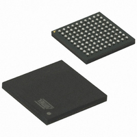
AT91SAM7XC512-CU Atmel, AT91SAM7XC512-CU Datasheet - Page 329

AT91SAM7XC512-CU
Manufacturer Part Number
AT91SAM7XC512-CU
Description
MCU ARM 512K HS FLASH 100-TFBGA
Manufacturer
Atmel
Series
AT91SAMr
Specifications of AT91SAM7XC512-CU
Core Processor
ARM7
Core Size
16/32-Bit
Speed
55MHz
Connectivity
CAN, Ethernet, I²C, SPI, SSC, UART/USART, USB
Peripherals
Brown-out Detect/Reset, DMA, POR, PWM, WDT
Number Of I /o
62
Program Memory Size
512KB (512K x 8)
Program Memory Type
FLASH
Ram Size
128K x 8
Voltage - Supply (vcc/vdd)
1.65 V ~ 1.95 V
Data Converters
A/D 8x10b
Oscillator Type
Internal
Operating Temperature
-40°C ~ 85°C
Package / Case
100-TFBGA
Processor Series
AT91SAMx
Core
ARM7TDMI
Data Bus Width
32 bit
Data Ram Size
128 KB
Interface Type
MII, SPI, TWI
Maximum Clock Frequency
55 MHz
Number Of Programmable I/os
62
Number Of Timers
3
Maximum Operating Temperature
+ 85 C
Mounting Style
SMD/SMT
3rd Party Development Tools
JTRACE-ARM-2M, KSK-AT91SAM7X-PL, MDK-ARM, RL-ARM, ULINK2
Development Tools By Supplier
AT91SAM-ICE, AT91-ISP, AT91SAM7XC-EK
Minimum Operating Temperature
- 40 C
On-chip Adc
10 bit, 8 Channel
For Use With
AT91SAM-ICE - EMULATOR FOR AT91 ARM7/ARM9AT91SAM7XC-EK - KIT EVAL FOR AT91SAM7XC256/128
Lead Free Status / RoHS Status
Lead free / RoHS Compliant
Eeprom Size
-
Lead Free Status / Rohs Status
Lead free / RoHS Compliant
Available stocks
Company
Part Number
Manufacturer
Quantity
Price
- Current page: 329 of 727
- Download datasheet (11Mb)
30.8.6
Name:
Access Type:
• DATLEN: Data Length
0: Forbidden value (1-bit data length not supported).
Any other value: The bit stream contains DATLEN + 1 data bits. Moreover, it defines the transfer size performed by the
PDC2 assigned to the Transmit. If DATLEN is lower or equal to 7, data transfers are bytes, if DATLEN is between 8 and 15
(included), half-words are transferred, and for any other value, 32-bit words are transferred.
• DATDEF: Data Default Value
This bit defines the level driven on the TD pin while out of transmission. Note that if the pin is defined as multi-drive by the
PIO Controller, the pin is enabled only if the SCC TD output is 1.
• MSBF: Most Significant Bit First
0: The lowest significant bit of the data register is shifted out first in the bit stream.
1: The most significant bit of the data register is shifted out first in the bit stream.
• DATNB: Data Number per frame
This field defines the number of data words to be transferred after each transfer start, which is equal to (DATNB +1).
• FSLEN: Transmit Frame Sync Length
This field defines the length of the Transmit Frame Sync signal and the number of bits shifted out from the Transmit Sync
Data Register if FSDEN is 1.
Pulse length is equal to (FSLEN + 1) Transmit Clock periods, i.e., the pulse length can range from 1 to 16 Transmit Clock
periods. If FSLEN is 0, the Transmit Frame Sync signal is generated during one Transmit Clock period.
6209F–ATARM–17-Feb-09
FSDEN
MSBF
31
23
15
–
–
7
SSC Transmit Frame Mode Register
30
22
14
SSC_TFMR
Read-write
–
–
6
–
DATDEF
FSOS
29
21
13
–
–
5
AT91SAM7XC512/256/128 Preliminary
28
20
12
–
–
4
27
19
11
–
3
DATLEN
26
18
10
–
2
FSLEN
DATNB
25
17
–
9
1
FSEDGE
24
16
8
0
329
Related parts for AT91SAM7XC512-CU
Image
Part Number
Description
Manufacturer
Datasheet
Request
R

Part Number:
Description:
KIT EVAL FOR AT91SAM7XC256/128
Manufacturer:
Atmel
Datasheet:

Part Number:
Description:
KIT EVAL FOR AT91SAM7X256/128
Manufacturer:
Atmel
Datasheet:

Part Number:
Description:
MCU, MPU & DSP Development Tools KICKSTART KIT ATMEL AT91SAM7X
Manufacturer:
IAR Systems

Part Number:
Description:
MCU ARM9 64K SRAM 144-LFBGA
Manufacturer:
Atmel
Datasheet:

Part Number:
Description:
IC ARM7 MCU FLASH 256K 100LQFP
Manufacturer:
Atmel
Datasheet:

Part Number:
Description:
IC ARM9 MPU 217-LFBGA
Manufacturer:
Atmel
Datasheet:

Part Number:
Description:
MCU ARM9 ULTRA LOW PWR 217-LFBGA
Manufacturer:
Atmel
Datasheet:

Part Number:
Description:
MCU ARM9 324-TFBGA
Manufacturer:
Atmel
Datasheet:

Part Number:
Description:
IC MCU ARM9 SAMPLING 217CBGA
Manufacturer:
Atmel
Datasheet:

Part Number:
Description:
IC ARM9 MCU 217-LFBGA
Manufacturer:
Atmel
Datasheet:

Part Number:
Description:
IC ARM9 MCU 208-PQFP
Manufacturer:
Atmel
Datasheet:

Part Number:
Description:
MCU ARM 512K HS FLASH 100-LQFP
Manufacturer:
Atmel
Datasheet:

Part Number:
Description:
MCU ARM 512K HS FLASH 100-TFBGA
Manufacturer:
Atmel
Datasheet:

Part Number:
Description:
IC ARM9 MCU 200 MHZ 324-TFBGA
Manufacturer:
Atmel
Datasheet:

Part Number:
Description:
IC ARM MCU 16BIT 128K 256BGA
Manufacturer:
Atmel
Datasheet:


