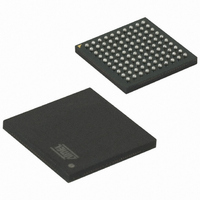
AT91SAM7XC512-CU Atmel, AT91SAM7XC512-CU Datasheet - Page 429

AT91SAM7XC512-CU
Manufacturer Part Number
AT91SAM7XC512-CU
Description
MCU ARM 512K HS FLASH 100-TFBGA
Manufacturer
Atmel
Series
AT91SAMr
Specifications of AT91SAM7XC512-CU
Core Processor
ARM7
Core Size
16/32-Bit
Speed
55MHz
Connectivity
CAN, Ethernet, I²C, SPI, SSC, UART/USART, USB
Peripherals
Brown-out Detect/Reset, DMA, POR, PWM, WDT
Number Of I /o
62
Program Memory Size
512KB (512K x 8)
Program Memory Type
FLASH
Ram Size
128K x 8
Voltage - Supply (vcc/vdd)
1.65 V ~ 1.95 V
Data Converters
A/D 8x10b
Oscillator Type
Internal
Operating Temperature
-40°C ~ 85°C
Package / Case
100-TFBGA
Processor Series
AT91SAMx
Core
ARM7TDMI
Data Bus Width
32 bit
Data Ram Size
128 KB
Interface Type
MII, SPI, TWI
Maximum Clock Frequency
55 MHz
Number Of Programmable I/os
62
Number Of Timers
3
Maximum Operating Temperature
+ 85 C
Mounting Style
SMD/SMT
3rd Party Development Tools
JTRACE-ARM-2M, KSK-AT91SAM7X-PL, MDK-ARM, RL-ARM, ULINK2
Development Tools By Supplier
AT91SAM-ICE, AT91-ISP, AT91SAM7XC-EK
Minimum Operating Temperature
- 40 C
On-chip Adc
10 bit, 8 Channel
For Use With
AT91SAM-ICE - EMULATOR FOR AT91 ARM7/ARM9AT91SAM7XC-EK - KIT EVAL FOR AT91SAM7XC256/128
Lead Free Status / RoHS Status
Lead free / RoHS Compliant
Eeprom Size
-
Lead Free Status / Rohs Status
Lead free / RoHS Compliant
Available stocks
Company
Part Number
Manufacturer
Quantity
Price
- Current page: 429 of 727
- Download datasheet (11Mb)
6209F–ATARM–17-Feb-09
Figure 33-4. Non Overlapped Center Aligned Waveforms
Note:
• the waveform duty cycle. This channel parameter is defined in the CDTY field of the
• the waveform polarity. At the beginning of the period, the signal can be at high or low level.
• the waveform alignment. The output waveform can be left or center aligned. Center aligned
By using a Master Clock divided by one of both DIVA or DIVB divider, the formula becomes,
respectively:
(
-------------------------------------------- -
If the waveform is center aligned then the output waveform period depends on the counter
source clock and can be calculated:
By using the Master Clock (MCK) divided by an X given prescaler value
(with X being 1, 2, 4, 8, 16, 32, 64, 128, 256, 512, or 1024). The resulting period formula will
be:
(
--------------------------------------------
By using a Master Clock divided by one of both DIVA or DIVB divider, the formula becomes,
respectively:
(
-------------------------------------------------------
PWM_CDTYx register.
If the waveform is left aligned then:
If the waveform is center aligned, then:
This property is defined in the CPOL field of the PWM_CMRx register. By default the signal
starts by a low level.
waveforms can be used to generate non overlapped waveforms. This property is defined in
the CALG field of the PWM_CMRx register. The default mode is left aligned.
CRPD
2
2
PWM0
PWM1
duty cycle
duty cycle
×
×
X
CPRD
See
MCK
MCK
×
MCK
×
CPRD
Figure 33-5 on page 431
DIVA
×
=
=
DIVA
No overlap
)
)
(
------------------------------------------------------------------------------------------------------------- -
(
-------------------------------------------------------------------------------------------------------------------------------- -
period 1
(
or
period
)
AT91SAM7XC512/256/128 Preliminary
(
------------------------------------------------ -
CRPD
or
Period
(
-------------------------------------------------------
–
2
⁄
MCK
×
×
2
⁄
CPRD
) 1
DIVAB
fchannel_x_clock
–
MCK
for a detailed description of center aligned waveforms.
period
⁄
(
×
period
)
fchannel_x_clock
DIVB
)
⁄
2
)
×
CDTY
×
CDTY
)
) )
429
Related parts for AT91SAM7XC512-CU
Image
Part Number
Description
Manufacturer
Datasheet
Request
R

Part Number:
Description:
KIT EVAL FOR AT91SAM7XC256/128
Manufacturer:
Atmel
Datasheet:

Part Number:
Description:
KIT EVAL FOR AT91SAM7X256/128
Manufacturer:
Atmel
Datasheet:

Part Number:
Description:
MCU, MPU & DSP Development Tools KICKSTART KIT ATMEL AT91SAM7X
Manufacturer:
IAR Systems

Part Number:
Description:
MCU ARM9 64K SRAM 144-LFBGA
Manufacturer:
Atmel
Datasheet:

Part Number:
Description:
IC ARM7 MCU FLASH 256K 100LQFP
Manufacturer:
Atmel
Datasheet:

Part Number:
Description:
IC ARM9 MPU 217-LFBGA
Manufacturer:
Atmel
Datasheet:

Part Number:
Description:
MCU ARM9 ULTRA LOW PWR 217-LFBGA
Manufacturer:
Atmel
Datasheet:

Part Number:
Description:
MCU ARM9 324-TFBGA
Manufacturer:
Atmel
Datasheet:

Part Number:
Description:
IC MCU ARM9 SAMPLING 217CBGA
Manufacturer:
Atmel
Datasheet:

Part Number:
Description:
IC ARM9 MCU 217-LFBGA
Manufacturer:
Atmel
Datasheet:

Part Number:
Description:
IC ARM9 MCU 208-PQFP
Manufacturer:
Atmel
Datasheet:

Part Number:
Description:
MCU ARM 512K HS FLASH 100-LQFP
Manufacturer:
Atmel
Datasheet:

Part Number:
Description:
MCU ARM 512K HS FLASH 100-TFBGA
Manufacturer:
Atmel
Datasheet:

Part Number:
Description:
IC ARM9 MCU 200 MHZ 324-TFBGA
Manufacturer:
Atmel
Datasheet:

Part Number:
Description:
IC ARM MCU 16BIT 128K 256BGA
Manufacturer:
Atmel
Datasheet:


