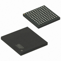
AT91SAM7XC512-CU Atmel, AT91SAM7XC512-CU Datasheet - Page 483

AT91SAM7XC512-CU
Manufacturer Part Number
AT91SAM7XC512-CU
Description
MCU ARM 512K HS FLASH 100-TFBGA
Manufacturer
Atmel
Series
AT91SAMr
Specifications of AT91SAM7XC512-CU
Core Processor
ARM7
Core Size
16/32-Bit
Speed
55MHz
Connectivity
CAN, Ethernet, I²C, SPI, SSC, UART/USART, USB
Peripherals
Brown-out Detect/Reset, DMA, POR, PWM, WDT
Number Of I /o
62
Program Memory Size
512KB (512K x 8)
Program Memory Type
FLASH
Ram Size
128K x 8
Voltage - Supply (vcc/vdd)
1.65 V ~ 1.95 V
Data Converters
A/D 8x10b
Oscillator Type
Internal
Operating Temperature
-40°C ~ 85°C
Package / Case
100-TFBGA
Processor Series
AT91SAMx
Core
ARM7TDMI
Data Bus Width
32 bit
Data Ram Size
128 KB
Interface Type
MII, SPI, TWI
Maximum Clock Frequency
55 MHz
Number Of Programmable I/os
62
Number Of Timers
3
Maximum Operating Temperature
+ 85 C
Mounting Style
SMD/SMT
3rd Party Development Tools
JTRACE-ARM-2M, KSK-AT91SAM7X-PL, MDK-ARM, RL-ARM, ULINK2
Development Tools By Supplier
AT91SAM-ICE, AT91-ISP, AT91SAM7XC-EK
Minimum Operating Temperature
- 40 C
On-chip Adc
10 bit, 8 Channel
For Use With
AT91SAM-ICE - EMULATOR FOR AT91 ARM7/ARM9AT91SAM7XC-EK - KIT EVAL FOR AT91SAM7XC256/128
Lead Free Status / RoHS Status
Lead free / RoHS Compliant
Eeprom Size
-
Lead Free Status / Rohs Status
Lead free / RoHS Compliant
Available stocks
Company
Part Number
Manufacturer
Quantity
Price
- Current page: 483 of 727
- Download datasheet (11Mb)
• RX_DATA_BK1: Receive Data Bank 1 (only used by endpoints with ping-pong attributes)
This flag generates an interrupt while it is set to one.
Write (Cleared by the firmware):
0 = Notifies USB device that data have been read in the FIFO’s Bank 1.
1 = No effect.
Read (Set by the USB peripheral):
0 = No data packet has been received in the FIFO's Bank 1.
1 = A data packet has been received, it has been stored in FIFO's Bank 1.
When the device firmware has polled this bit or has been interrupted by this signal, it must transfer data from the FIFO to
microcontroller memory. The number of bytes received is available in RXBYTECNT field. Bank 1 FIFO values are read
through UDP_ FDRx register. Once a transfer is done, the device firmware must release Bank 1 to the USB device by
clearing RX_DATA_BK1.
• DIR: Transfer Direction (only available for control endpoints)
Read/Write
0 = Allows Data OUT transactions in the control data stage.
1 = Enables Data IN transactions in the control data stage.
Refer to Chapter 8.5.3 of the Universal Serial Bus Specification, Rev. 2.0 for more information on the control data stage.
This bit must be set before UDP_ CSRx/RXSETUP is cleared at the end of the setup stage. According to the request sent
in the setup data packet, the data stage is either a device to host (DIR = 1) or host to device (DIR = 0) data transfer. It is not
necessary to check this bit to reverse direction for the status stage.
• EPTYPE[2:0]: Endpoint Type
Read/Write
• DTGLE: Data Toggle
Read-only
0 = Identifies DATA0 packet.
1 = Identifies DATA1 packet.
Refer to Chapter 8 of the Universal Serial Bus Specification, Rev. 2.0 for more information on DATA0, DATA1 packet
definitions.
6209F–ATARM–17-Feb-09
000
001
101
010
110
011
111
Control
Isochronous OUT
Isochronous IN
Bulk OUT
Bulk IN
Interrupt OUT
Interrupt IN
AT91SAM7XC512/256/128 Preliminary
483
Related parts for AT91SAM7XC512-CU
Image
Part Number
Description
Manufacturer
Datasheet
Request
R

Part Number:
Description:
KIT EVAL FOR AT91SAM7XC256/128
Manufacturer:
Atmel
Datasheet:

Part Number:
Description:
KIT EVAL FOR AT91SAM7X256/128
Manufacturer:
Atmel
Datasheet:

Part Number:
Description:
MCU, MPU & DSP Development Tools KICKSTART KIT ATMEL AT91SAM7X
Manufacturer:
IAR Systems

Part Number:
Description:
MCU ARM9 64K SRAM 144-LFBGA
Manufacturer:
Atmel
Datasheet:

Part Number:
Description:
IC ARM7 MCU FLASH 256K 100LQFP
Manufacturer:
Atmel
Datasheet:

Part Number:
Description:
IC ARM9 MPU 217-LFBGA
Manufacturer:
Atmel
Datasheet:

Part Number:
Description:
MCU ARM9 ULTRA LOW PWR 217-LFBGA
Manufacturer:
Atmel
Datasheet:

Part Number:
Description:
MCU ARM9 324-TFBGA
Manufacturer:
Atmel
Datasheet:

Part Number:
Description:
IC MCU ARM9 SAMPLING 217CBGA
Manufacturer:
Atmel
Datasheet:

Part Number:
Description:
IC ARM9 MCU 217-LFBGA
Manufacturer:
Atmel
Datasheet:

Part Number:
Description:
IC ARM9 MCU 208-PQFP
Manufacturer:
Atmel
Datasheet:

Part Number:
Description:
MCU ARM 512K HS FLASH 100-LQFP
Manufacturer:
Atmel
Datasheet:

Part Number:
Description:
MCU ARM 512K HS FLASH 100-TFBGA
Manufacturer:
Atmel
Datasheet:

Part Number:
Description:
IC ARM9 MCU 200 MHZ 324-TFBGA
Manufacturer:
Atmel
Datasheet:

Part Number:
Description:
IC ARM MCU 16BIT 128K 256BGA
Manufacturer:
Atmel
Datasheet:


