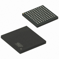
AT91SAM7XC512-CU Atmel, AT91SAM7XC512-CU Datasheet - Page 714

AT91SAM7XC512-CU
Manufacturer Part Number
AT91SAM7XC512-CU
Description
MCU ARM 512K HS FLASH 100-TFBGA
Manufacturer
Atmel
Series
AT91SAMr
Specifications of AT91SAM7XC512-CU
Core Processor
ARM7
Core Size
16/32-Bit
Speed
55MHz
Connectivity
CAN, Ethernet, I²C, SPI, SSC, UART/USART, USB
Peripherals
Brown-out Detect/Reset, DMA, POR, PWM, WDT
Number Of I /o
62
Program Memory Size
512KB (512K x 8)
Program Memory Type
FLASH
Ram Size
128K x 8
Voltage - Supply (vcc/vdd)
1.65 V ~ 1.95 V
Data Converters
A/D 8x10b
Oscillator Type
Internal
Operating Temperature
-40°C ~ 85°C
Package / Case
100-TFBGA
Processor Series
AT91SAMx
Core
ARM7TDMI
Data Bus Width
32 bit
Data Ram Size
128 KB
Interface Type
MII, SPI, TWI
Maximum Clock Frequency
55 MHz
Number Of Programmable I/os
62
Number Of Timers
3
Maximum Operating Temperature
+ 85 C
Mounting Style
SMD/SMT
3rd Party Development Tools
JTRACE-ARM-2M, KSK-AT91SAM7X-PL, MDK-ARM, RL-ARM, ULINK2
Development Tools By Supplier
AT91SAM-ICE, AT91-ISP, AT91SAM7XC-EK
Minimum Operating Temperature
- 40 C
On-chip Adc
10 bit, 8 Channel
For Use With
AT91SAM-ICE - EMULATOR FOR AT91 ARM7/ARM9AT91SAM7XC-EK - KIT EVAL FOR AT91SAM7XC256/128
Lead Free Status / RoHS Status
Lead free / RoHS Compliant
Eeprom Size
-
Lead Free Status / Rohs Status
Lead free / RoHS Compliant
Available stocks
Company
Part Number
Manufacturer
Quantity
Price
- Current page: 714 of 727
- Download datasheet (11Mb)
714
Version
6209D
(Continued)
AT91SAM7XC512/256/128 Preliminary
Comments
SPI:
location defined.
Section 28.7.4 “SPI Transmit Data Register” on page
Section 28.7.2 “SPI Mode Register” on page
Updated
28.7.2 “SPI Mode Register” on page 269
LLB description modified in
Updated
Updated information on SPI_RDR in
information to SWRST bit description in
equations in DLYBCT bit description,
Changes to
TWI:
Registers.
USART:
MANCHESTER FUNCTIONALITY REMOVED.
Section 30.5.1 “I/O Lines” on page
Section 30.6.1.3 “Fractional Baud Rate in Asynchronous Mode” on page
“functional mode” changed to USART “normal mode”.
Table 30-3, “Binary and Decimal Values for Di,” on page 307
Values for Fi,” on page
Figure 30-25, ”IrDA Demodulator Operations” on page 323
Section 30.6.4.1 “ISO7816 Mode Overview” on page 319
Section 30.6.7 “Modem Mode” on page 325
Table 30-2, “Baud Rate Example (OVER = 0),” on page 304
clocks removed.
Section 30.6.3.2 ”Asynchronous Receiver”
synchronization Mechanism......”
Section 30.6.3.8 ”Receiver Time-out”
Section 30.7.1 ”USART Control Register”
Section 30.7.6 ”USART Channel Status Register”
register
TC:
longer used as an output and the compare register B is not used to generate waveforms and
subsequently no IRQs. Note
Channel Mode Register: Waveform Mode” on page 367
PWM:
generation.
Section 31.5.3.6 “External Event/Trigger Conditions” on page 359
Section 28.7.5 “SPI Status Register” on page 273
Section 29.6 ”TWI User
Section 32.5.3.3 ”Changing the Duty Cycle or the
Figure 28-1, ”Block Diagram” on page
Figure 28-9, ”Slave Mode Functional Block Diagram” on page 266
Section 28.6.3.8 “Mode Fault Detection” on page
307: DI and Fi properly referenced in titles.
Section 28.7.2 “SPI Mode Register” on page
(1)
Interface”: OVRE and UNRE bit fields removed from Status and Interrupt
attached to ”EEVT: External Event Selection” in
302, text concerning TXD line added.
Section 28.6.3 “Master Mode Operations” on page
Section 28.7.9 ”SPI Chip Select Register”
list of user options rewritten.
Section 28.7.1 “SPI Control Register” on page
and
STTTO bit function related to TIMEOUT in US_CSR register
changed 2nd sentence in 4th paragraph “For the
Control of DTR and RTS output pins.
269,
Section 28.7.9 “SPI Chip Select Register” on page
256, removed Note. Removed bit FDIV from
PCSDEC: Chip Select Decode
TIMEOUT bit function related to STTTO in US_CR
272,
SPI_RCR, SPI_RNCR, SPI_TCR, SPI_TNCR
further clarifies this condition.
Period”: updated info on waveform
clarification of PAR configuration added.
LASTXFER: Last Transfer
modified.
lines showing over 50 000 000 MHz
and
265.
Table 30-4, “Binary and Decimal
“....(EEVT = 0), TIOB is no
305, using USART
269.
to remove FLOAD.
on
Section 31.6.7 “TC
page
changed.
268. Corrected
260. Added
279.
text added.
Section
278.
6209F–ATARM–17-Feb-09
Change
Request
Ref.
04-183
05-434
05-476
05-484
1542
1543
1676
2470
#2768
1552
1770
2942
3023
2704
1677
Related parts for AT91SAM7XC512-CU
Image
Part Number
Description
Manufacturer
Datasheet
Request
R

Part Number:
Description:
KIT EVAL FOR AT91SAM7XC256/128
Manufacturer:
Atmel
Datasheet:

Part Number:
Description:
KIT EVAL FOR AT91SAM7X256/128
Manufacturer:
Atmel
Datasheet:

Part Number:
Description:
MCU, MPU & DSP Development Tools KICKSTART KIT ATMEL AT91SAM7X
Manufacturer:
IAR Systems

Part Number:
Description:
MCU ARM9 64K SRAM 144-LFBGA
Manufacturer:
Atmel
Datasheet:

Part Number:
Description:
IC ARM7 MCU FLASH 256K 100LQFP
Manufacturer:
Atmel
Datasheet:

Part Number:
Description:
IC ARM9 MPU 217-LFBGA
Manufacturer:
Atmel
Datasheet:

Part Number:
Description:
MCU ARM9 ULTRA LOW PWR 217-LFBGA
Manufacturer:
Atmel
Datasheet:

Part Number:
Description:
MCU ARM9 324-TFBGA
Manufacturer:
Atmel
Datasheet:

Part Number:
Description:
IC MCU ARM9 SAMPLING 217CBGA
Manufacturer:
Atmel
Datasheet:

Part Number:
Description:
IC ARM9 MCU 217-LFBGA
Manufacturer:
Atmel
Datasheet:

Part Number:
Description:
IC ARM9 MCU 208-PQFP
Manufacturer:
Atmel
Datasheet:

Part Number:
Description:
MCU ARM 512K HS FLASH 100-LQFP
Manufacturer:
Atmel
Datasheet:

Part Number:
Description:
MCU ARM 512K HS FLASH 100-TFBGA
Manufacturer:
Atmel
Datasheet:

Part Number:
Description:
IC ARM9 MCU 200 MHZ 324-TFBGA
Manufacturer:
Atmel
Datasheet:

Part Number:
Description:
IC ARM MCU 16BIT 128K 256BGA
Manufacturer:
Atmel
Datasheet:


