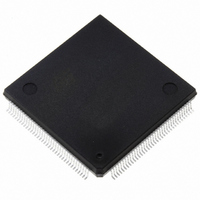
ST10F269Z2Q3 STMicroelectronics, ST10F269Z2Q3 Datasheet - Page 151

ST10F269Z2Q3
Manufacturer Part Number
ST10F269Z2Q3
Description
IC FLASH MEM 256KBIT 144-PQFP
Manufacturer
STMicroelectronics
Series
ST10r
Datasheet
1.ST10F269Z2Q3.pdf
(184 pages)
Specifications of ST10F269Z2Q3
Core Processor
ST10
Core Size
16-Bit
Speed
40MHz
Connectivity
CAN, EBI/EMI, SSC, UART/USART
Peripherals
POR, PWM, WDT
Number Of I /o
111
Program Memory Size
256KB (256K x 8)
Program Memory Type
FLASH
Ram Size
12K x 8
Voltage - Supply (vcc/vdd)
4.5 V ~ 5.5 V
Data Converters
A/D 16x10b
Oscillator Type
Internal
Operating Temperature
-40°C ~ 125°C
Package / Case
144-QFP
Processor Series
ST10F26x
Core
ST10
Data Bus Width
16 bit
Data Ram Size
12 KB
Interface Type
CAN, SSC, USART
Maximum Clock Frequency
40 MHz
Number Of Programmable I/os
111
Number Of Timers
2 x 16 bit
Operating Supply Voltage
0.3 V to 4 V
Maximum Operating Temperature
+ 125 C
Mounting Style
SMD/SMT
Minimum Operating Temperature
- 40 C
On-chip Adc
16 bit x 10 bit
Cpu Family
ST10
Device Core Size
16b
Frequency (max)
40MHz
Total Internal Ram Size
12KB
# I/os (max)
111
Number Of Timers - General Purpose
5
Operating Supply Voltage (typ)
5V
Operating Supply Voltage (max)
5.5V
Operating Supply Voltage (min)
4.5V
Instruction Set Architecture
CISC/RISC
Operating Temp Range
-40C to 125C
Operating Temperature Classification
Automotive
Mounting
Surface Mount
Pin Count
144
Package Type
PQFP
Lead Free Status / RoHS Status
Lead free / RoHS Compliant
Eeprom Size
-
Lead Free Status / Rohs Status
Lead free / RoHS Compliant
Other names
497-2042
Available stocks
Company
Part Number
Manufacturer
Quantity
Price
Company:
Part Number:
ST10F269Z2Q3
Manufacturer:
INFINEON
Quantity:
1 443
Company:
Part Number:
ST10F269Z2Q3
Manufacturer:
STMicroelectronics
Quantity:
10 000
Part Number:
ST10F269Z2Q3
Manufacturer:
ST
Quantity:
20 000
ST10F269
V
1. Theoretical minimum. The real minimum value depends on the duty cycle of the input clock signal. 32MHz is the maximum input frequency
when using an external crystal oscillator. However, 32MHz can be applied with an external clock source.
2. The input clock signal must reach the defined levels V
Figure 70 : External Clock Drive XTAL1
21.4.9 - Memory Cycle Variables
The tables below use three variables which are derived from the BUSCONx registers and represent the
special characteristics of the programmed memory cycle. The following table describes, how these
variables are to be computed.
Oscillator period
High time
Low time
Rise time
Fall time
ALE Extension
Memory Cycle Time wait states
Memory Tri-state Time
DD
= 5V
Parameter
10%, V
Description
SS
t
t
t
t
t
= 0V, T
OSC
1
2
3
4
Symbol
SR
SR
SR
SR
SR
A
= -40 to +125 °C (TQFP144 devices)
t
Minimum
1
31.25
12.5
12.5
–
–
f
CPU
2
2
1
= f
IL
Symbol
Maximum
and V
XTAL
V
3.125
3.125
IH2
t
t
t
A
C
F
–
–
–
IH2
2
2
t
.
2
t
3
Minimum
15.625
TCL x [ALECTL]
2TCL x (15 - [MCTC])
2TCL x (1 - [MTTC])
6.25
6.25
f
CPU
–
–
t
2
2
OSC
V
= f
IL
XTAL
Maximum Minimum Maximum
1.56
1.56
/ 2
–
–
–
2
2
Values
31.25 x N
F = 1.5/2,/2.5/3/4/5
12.5
12.5
f
CPU
–
–
2
2
= f
t
4
XTAL
3.125
3.125
x F
–
–
–
2
2
151/184
Unit
ns
ns
ns
ns
ns


