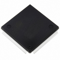
ST10F269Z2Q3 STMicroelectronics, ST10F269Z2Q3 Datasheet - Page 162

ST10F269Z2Q3
Manufacturer Part Number
ST10F269Z2Q3
Description
IC FLASH MEM 256KBIT 144-PQFP
Manufacturer
STMicroelectronics
Series
ST10r
Datasheet
1.ST10F269Z2Q3.pdf
(184 pages)
Specifications of ST10F269Z2Q3
Core Processor
ST10
Core Size
16-Bit
Speed
40MHz
Connectivity
CAN, EBI/EMI, SSC, UART/USART
Peripherals
POR, PWM, WDT
Number Of I /o
111
Program Memory Size
256KB (256K x 8)
Program Memory Type
FLASH
Ram Size
12K x 8
Voltage - Supply (vcc/vdd)
4.5 V ~ 5.5 V
Data Converters
A/D 16x10b
Oscillator Type
Internal
Operating Temperature
-40°C ~ 125°C
Package / Case
144-QFP
Processor Series
ST10F26x
Core
ST10
Data Bus Width
16 bit
Data Ram Size
12 KB
Interface Type
CAN, SSC, USART
Maximum Clock Frequency
40 MHz
Number Of Programmable I/os
111
Number Of Timers
2 x 16 bit
Operating Supply Voltage
0.3 V to 4 V
Maximum Operating Temperature
+ 125 C
Mounting Style
SMD/SMT
Minimum Operating Temperature
- 40 C
On-chip Adc
16 bit x 10 bit
Cpu Family
ST10
Device Core Size
16b
Frequency (max)
40MHz
Total Internal Ram Size
12KB
# I/os (max)
111
Number Of Timers - General Purpose
5
Operating Supply Voltage (typ)
5V
Operating Supply Voltage (max)
5.5V
Operating Supply Voltage (min)
4.5V
Instruction Set Architecture
CISC/RISC
Operating Temp Range
-40C to 125C
Operating Temperature Classification
Automotive
Mounting
Surface Mount
Pin Count
144
Package Type
PQFP
Lead Free Status / RoHS Status
Lead free / RoHS Compliant
Eeprom Size
-
Lead Free Status / Rohs Status
Lead free / RoHS Compliant
Other names
497-2042
Available stocks
Company
Part Number
Manufacturer
Quantity
Price
Company:
Part Number:
ST10F269Z2Q3
Manufacturer:
INFINEON
Quantity:
1 443
Company:
Part Number:
ST10F269Z2Q3
Manufacturer:
STMicroelectronics
Quantity:
10 000
Part Number:
ST10F269Z2Q3
Manufacturer:
ST
Quantity:
20 000
162/184
t
t
t
t
t
t
t
t
t
t
t
t
t
t
t
t
t
t
t
t
t
t
81
12
13
14
15
16
17
18
20
21
22
24
26
28
28h
38
39
41
82
83
46
47
Symbol
CC
CC
CC
SR
SR
SR
SR
SR
SR
SR
CC
CC
CC
CC
CC
CC
SR
CC
CC
CC
SR
SR
Address/Unlatched CS setup
to RD, WR
(no RW-delay)
RD, WR low time
RD, WR low time
RD to valid data in
RD to valid data in
ALE low to valid data in
Address/Unlatched CS to
valid data in
Data hold after RD
rising edge
Data float after RD rising
edge (with RW-delay)
Data float after RD rising
edge (no RW-delay)
Data valid to WR
Data hold after WR
ALE rising edge after RD, WR
Address/Unlatched CS hold
after RD, WR
Address/Unlatched CS hold
after WRH
ALE falling edge to Latched
CS
Latched CS low to Valid Data
In
Latched CS hold after RD,
WR
Address setup to RdCS,
WrCS
(with RW-delay)
Address setup to RdCS,
WrCS
(no RW-delay)
RdCS to Valid Data In
(with RW-delay)
RdCS to Valid Data In
(no RW-delay)
(with RW-delay)
(no RW-delay)
(with RW-delay)
(no RW-delay)
Parameter
2
1 - 3
1 - 3
36.875 + t
5.625 + 2t
17.25 + 2t
1.625 + 2t
21.25 + t
11.25 + t
5.625 + t
1.625 + t
Minimum
Maximum CPU Clock =
0 (no t
(t
-10 + t
-5 + t
-5 + t
-4 - t
F
–
–
–
–
0
–
–
–
–
–
> 0)
F
A
F
F
F
)
C
C
F
F
32MHz
A
C
A
A
26.875 + t
26.875 + t
32.5 + 2t
26.875 + t
22.875 + t
Maximum
11.25 + t
5.625 + t
7.25 + t
26 + t
10 - t
2t
t
t
–
–
–
–
–
–
–
–
–
–
–
–
C
C
A
A
F
A
C
A
C
C
F
C
C
+
+
+
2TCL - 14 + 2t
2TCL - 10 + t
3TCL - 10 + t
2TCL- 20 + t
TCL -10 + 2t
TCL -14 + 2t
TCL - 14 + t
TCL - 10+ t
Minimum
0 (no t
(t
-10 + t
-5 + t
-5 + t
-4 - t
1/2 TCL = 1 to 32MHz
F
Variable CPU Clock
–
–
–
–
0
–
–
–
–
–
> 0)
A
F
F
F
F
)
F
F
A
C
A
C
C
A
2TCL - 20 + t
3TCL - 20 + t
2TCL - 24 + t
3TCL - 24 + t
+ t
+ t
Maximum
3TCL - 20
4TCL - 30
+ 2t
2TCL - 14
3TCL - 20
+ t
TCL - 10
+ t
10 - t
F
F
C
A
A
+ 2t
+ 2t
–
–
–
–
–
–
–
–
–
–
–
–
+ 2t
+ t
+ t
ST10F269
A
C
A
A
C
A
1
1
C
C
C
C
Unit
ns
ns
ns
ns
ns
ns
ns
ns
ns
ns
ns
ns
ns
ns
ns
ns
ns
ns
ns
ns
ns
ns


