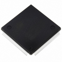
ST10F269Z2Q3 STMicroelectronics, ST10F269Z2Q3 Datasheet - Page 60

ST10F269Z2Q3
Manufacturer Part Number
ST10F269Z2Q3
Description
IC FLASH MEM 256KBIT 144-PQFP
Manufacturer
STMicroelectronics
Series
ST10r
Datasheet
1.ST10F269Z2Q3.pdf
(184 pages)
Specifications of ST10F269Z2Q3
Core Processor
ST10
Core Size
16-Bit
Speed
40MHz
Connectivity
CAN, EBI/EMI, SSC, UART/USART
Peripherals
POR, PWM, WDT
Number Of I /o
111
Program Memory Size
256KB (256K x 8)
Program Memory Type
FLASH
Ram Size
12K x 8
Voltage - Supply (vcc/vdd)
4.5 V ~ 5.5 V
Data Converters
A/D 16x10b
Oscillator Type
Internal
Operating Temperature
-40°C ~ 125°C
Package / Case
144-QFP
Processor Series
ST10F26x
Core
ST10
Data Bus Width
16 bit
Data Ram Size
12 KB
Interface Type
CAN, SSC, USART
Maximum Clock Frequency
40 MHz
Number Of Programmable I/os
111
Number Of Timers
2 x 16 bit
Operating Supply Voltage
0.3 V to 4 V
Maximum Operating Temperature
+ 125 C
Mounting Style
SMD/SMT
Minimum Operating Temperature
- 40 C
On-chip Adc
16 bit x 10 bit
Cpu Family
ST10
Device Core Size
16b
Frequency (max)
40MHz
Total Internal Ram Size
12KB
# I/os (max)
111
Number Of Timers - General Purpose
5
Operating Supply Voltage (typ)
5V
Operating Supply Voltage (max)
5.5V
Operating Supply Voltage (min)
4.5V
Instruction Set Architecture
CISC/RISC
Operating Temp Range
-40C to 125C
Operating Temperature Classification
Automotive
Mounting
Surface Mount
Pin Count
144
Package Type
PQFP
Lead Free Status / RoHS Status
Lead free / RoHS Compliant
Eeprom Size
-
Lead Free Status / Rohs Status
Lead free / RoHS Compliant
Other names
497-2042
Available stocks
Company
Part Number
Manufacturer
Quantity
Price
Company:
Part Number:
ST10F269Z2Q3
Manufacturer:
INFINEON
Quantity:
1 443
Company:
Part Number:
ST10F269Z2Q3
Manufacturer:
STMicroelectronics
Quantity:
10 000
Part Number:
ST10F269Z2Q3
Manufacturer:
ST
Quantity:
20 000
12 - PARALLEL PORTS
Figure 20 : Hysteresis for Special Input Thresholds
12.2.3 - Output Driver Control
The port output control registers POCONx allow
to select the port output driver characteristics of a
port. The aim of these selections is to adapt the
output drivers to the application’s requirements,
and to improve the EMI behaviour of the device.
Two characteristics may be selected:
Edge characteristic defines the rise/fall time for
the respective output. Slow edges reduce the
peak currents that are sinked/sourced when
changing the voltage level of an external
capacitive load. For a bus interface or pins that are
changing
however, fast edges may still be required.
Driver characteristic defines either the general
driving capability of the respective driver, or if the
POCONx (F0yyh / zzh) for 8-bit Ports
POCONx (F0yyh / zzh) for 16-bit Ports
Note: In case of reading an 8 bit P0CONX register, high Byte (bit 15..8) is read as 00h
60/184
PNxEC
PNxDC
15
15
-
PN3DC
RW
Bit
Hysteresis
Input level
Bit state
14
14
-
at frequency higher than
13
13
-
PN3EC
Port Nibble x Edge Characteristic (rise/fall time)
00:
01:
10:
11:
Port Nibble x Driver Characteristic (output current)
00:
01:
10:
11:
RW
12
12
-
Fast edge mode, rise/fall times depend on the size of the driver.
Slow edge mode, rise/fall times ~60 ns
Reserved
Reserved
High Current mode:
Driver always operates with maximum strength.
Dynamic Current mode:
Driver strength is reduced after the target level has been reached.
Low Current mode:
Driver always operates with reduced strength.
Reserved
11
11
-
PN2DC
RW
10
10
-
9
9
-
PN2EC
1MHz,
RW
8
8
-
ESFR
ESFR
driver strength is reduced after the target output
level has been reached or not. Reducing the
driver strength increases the output’s internal
resistance, which
imported via the output line. For driving LEDs or
power transistors, however, a stable high output
current may still be required as described below.
This rise / fall time of 4 I/O pads (a nibble) is
selected using 2-bit named PNxEC. That means
Port Nibble (x = nibble number, it could be 3 as for
Port 2.15 to 2.12) Edge Characteristic.
The sink / source capability of the same 4 I/O
pads is selected using 2-bit named PNxDC. That
means Port Nibble (x = nibble number) Drive
Characteristic (See Table 18).
7
7
PN1DC
PN1DC
Function
RW
RW
6
6
5
5
PN1EC
PN1EC
RW
RW
4
4
attenuates
3
3
PN0DC
PN0DC
RW
RW
Reset Value: 0000h
Reset Value: --00h
2
2
noise
ST10F269
1
1
PN0EC
PN0EC
RW
RW
that
0
0
is


