MC9S12C32CFAE25 Freescale Semiconductor, MC9S12C32CFAE25 Datasheet - Page 121
MC9S12C32CFAE25
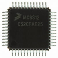
Manufacturer Part Number
MC9S12C32CFAE25
Description
IC MCU 32K FLASH 25MHZ 48-LQFP
Manufacturer
Freescale Semiconductor
Series
HCS12r
Datasheets
1.MC9S12GC16MFUE.pdf
(690 pages)
2.MC9S12C96CFUER.pdf
(26 pages)
3.MC9S12C32CFAE25.pdf
(2 pages)
4.MC9S12C32CPBE25.pdf
(36 pages)
Specifications of MC9S12C32CFAE25
Core Processor
HCS12
Core Size
16-Bit
Speed
25MHz
Connectivity
CAN, EBI/EMI, SCI, SPI
Peripherals
POR, PWM, WDT
Number Of I /o
31
Program Memory Size
32KB (32K x 8)
Program Memory Type
FLASH
Ram Size
2K x 8
Voltage - Supply (vcc/vdd)
2.35 V ~ 5.5 V
Data Converters
A/D 8x10b
Oscillator Type
Internal
Operating Temperature
-40°C ~ 85°C
Package / Case
48-LQFP
Processor Series
S12C
Core
HCS12
Data Bus Width
16 bit
Data Ram Size
2 KB
Interface Type
CAN/SCI/SPI
Maximum Clock Frequency
25 MHz
Number Of Programmable I/os
31
Number Of Timers
8
Maximum Operating Temperature
+ 85 C
Mounting Style
SMD/SMT
3rd Party Development Tools
EWHCS12
Development Tools By Supplier
M68EVB912C32EE
Minimum Operating Temperature
- 40 C
On-chip Adc
8-ch x 10-bit
For Use With
CML12C32SLK - KIT STUDENT LEARNING 16BIT HCS12
Lead Free Status / RoHS Status
Lead free / RoHS Compliant
Eeprom Size
-
Lead Free Status / Rohs Status
Lead free / RoHS Compliant
Available stocks
Company
Part Number
Manufacturer
Quantity
Price
Company:

Part Number:
MC9S12C32CFAE25
Manufacturer:
FREESCAL
Quantity:
240
Company:
Part Number:
MC9S12C32CFAE25
Manufacturer:
Freescale Semiconductor
Quantity:
10 000


3.3.2.9
Read: Anytime
Write: Determined at chip integration. Generally it’s: “write anytime in all modes;” on some devices it will
be: “write only in special modes.” Check specific device documentation to determine which applies.
Reset: Defined at chip integration as either 0x00 (paired with write in any mode) or 0x3C (paired with
write only in special modes), see device overview chapter.
The HCS12 core architecture limits the physical address space available to 64K bytes. The program page
index register allows for integrating up to 1M byte of FLASH or ROM into the system by using the six
page index bits to page 16K byte blocks into the program page window located from 0x8000 to 0xBFFF
as defined in
without using the address bus.
Freescale Semiconductor
Module Base + 0x0030
Starting address location affected by INITRG register setting.
1. The reset state of this register is controlled at chip integration. Please refer to the device overview section to determine the
Reset
actual reset state of this register.
PIX[5:0]
Field
5:0
W
R
1
Table
Program Page Index Register (PPAGE)
—
0
Program Page Index Bits 5:0 — These page index bits are used to select which of the 64 FLASH or ROM
array pages is to be accessed in the program page window as shown in
7
Normal writes to this register take one cycle to go into effect. Writes to this
register using the special access of the CALL and RTC instructions will be
complete before the end of the associated instruction.
3-14. CALL and RTC instructions have special access to read and write this register
= Unimplemented or Reserved
—
0
6
Figure 3-11. Program Page Index Register (PPAGE)
Table 3-13. MEMSIZ0 Field Descriptions
MC9S12C-Family / MC9S12GC-Family
PIX5
—
5
Rev 01.24
PIX4
NOTE
—
4
Description
Chapter 3 Module Mapping Control (MMCV4) Block Description
PIX3
—
3
PIX2
Table
—
2
3-14.
PIX1
—
1
PIX0
—
0
121
Related parts for MC9S12C32CFAE25
Image
Part Number
Description
Manufacturer
Datasheet
Request
R

Part Number:
Description:
Manufacturer:
Freescale Semiconductor, Inc
Datasheet:
Part Number:
Description:
Manufacturer:
Freescale Semiconductor, Inc
Datasheet:
Part Number:
Description:
Manufacturer:
Freescale Semiconductor, Inc
Datasheet:
Part Number:
Description:
Manufacturer:
Freescale Semiconductor, Inc
Datasheet:
Part Number:
Description:
Manufacturer:
Freescale Semiconductor, Inc
Datasheet:
Part Number:
Description:
Manufacturer:
Freescale Semiconductor, Inc
Datasheet:
Part Number:
Description:
Manufacturer:
Freescale Semiconductor, Inc
Datasheet:
Part Number:
Description:
Manufacturer:
Freescale Semiconductor, Inc
Datasheet:
Part Number:
Description:
Manufacturer:
Freescale Semiconductor, Inc
Datasheet:
Part Number:
Description:
Manufacturer:
Freescale Semiconductor, Inc
Datasheet:
Part Number:
Description:
Manufacturer:
Freescale Semiconductor, Inc
Datasheet:
Part Number:
Description:
Manufacturer:
Freescale Semiconductor, Inc
Datasheet:
Part Number:
Description:
Manufacturer:
Freescale Semiconductor, Inc
Datasheet:
Part Number:
Description:
Manufacturer:
Freescale Semiconductor, Inc
Datasheet:
Part Number:
Description:
Manufacturer:
Freescale Semiconductor, Inc
Datasheet: