MC9S12C32CFAE25 Freescale Semiconductor, MC9S12C32CFAE25 Datasheet - Page 619
MC9S12C32CFAE25
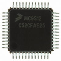
Manufacturer Part Number
MC9S12C32CFAE25
Description
IC MCU 32K FLASH 25MHZ 48-LQFP
Manufacturer
Freescale Semiconductor
Series
HCS12r
Datasheets
1.MC9S12GC16MFUE.pdf
(690 pages)
2.MC9S12C96CFUER.pdf
(26 pages)
3.MC9S12C32CFAE25.pdf
(2 pages)
4.MC9S12C32CPBE25.pdf
(36 pages)
Specifications of MC9S12C32CFAE25
Core Processor
HCS12
Core Size
16-Bit
Speed
25MHz
Connectivity
CAN, EBI/EMI, SCI, SPI
Peripherals
POR, PWM, WDT
Number Of I /o
31
Program Memory Size
32KB (32K x 8)
Program Memory Type
FLASH
Ram Size
2K x 8
Voltage - Supply (vcc/vdd)
2.35 V ~ 5.5 V
Data Converters
A/D 8x10b
Oscillator Type
Internal
Operating Temperature
-40°C ~ 85°C
Package / Case
48-LQFP
Processor Series
S12C
Core
HCS12
Data Bus Width
16 bit
Data Ram Size
2 KB
Interface Type
CAN/SCI/SPI
Maximum Clock Frequency
25 MHz
Number Of Programmable I/os
31
Number Of Timers
8
Maximum Operating Temperature
+ 85 C
Mounting Style
SMD/SMT
3rd Party Development Tools
EWHCS12
Development Tools By Supplier
M68EVB912C32EE
Minimum Operating Temperature
- 40 C
On-chip Adc
8-ch x 10-bit
For Use With
CML12C32SLK - KIT STUDENT LEARNING 16BIT HCS12
Lead Free Status / RoHS Status
Lead free / RoHS Compliant
Eeprom Size
-
Lead Free Status / Rohs Status
Lead free / RoHS Compliant
Available stocks
Company
Part Number
Manufacturer
Quantity
Price
Company:

Part Number:
MC9S12C32CFAE25
Manufacturer:
FREESCAL
Quantity:
240
Company:
Part Number:
MC9S12C32CFAE25
Manufacturer:
Freescale Semiconductor
Quantity:
10 000


21.3.2.1
The FCLKDIV register is used to control timed events in program and erase algorithms.
All bits in the FCLKDIV register are readable, bits 6–0 are write once and bit 7 is not writable.
21.3.2.2
The FSEC register holds all bits associated with the security of the MCU and Flash module.
All bits in the FSEC register are readable but not writable.
The FSEC register is loaded from the Flash configuration field at 0xFF0F during the reset sequence,
indicated by F in
Freescale Semiconductor
Module Base + 0x0000
Module Base + 0x0001
FDIV[5:0]
FDIVLD
PRDIV8
Reset
Reset
Field
5–0
7
6
W
W
R
R
KEYEN1
FDIVLD
Clock Divider Loaded
0 FCLKDIV register has not been written
1 FCLKDIV register has been written to since the last reset
Enable Prescalar by 8
0 The oscillator clock is directly fed into the Flash clock divider
1 The oscillator clock is divided by 8 before feeding into the Flash clock divider
Clock Divider Bits — The combination of PRDIV8 and FDIV[5:0] must divide the oscillator clock down to a
frequency of 150 kHz – 200 kHz. The maximum divide ratio is 512. Refer to
FCLKDIV Register”
Flash Clock Divider Register (FCLKDIV)
Flash Security Register (FSEC)
F
0
7
7
Figure
= Unimplemented or Reserved
= Unimplemented or Reserved
KEYEN0
PRDIV8
21-5.
0
F
6
6
Figure 21-4. Flash Clock Divider Register (FCLKDIV)
for more information.
Figure 21-5. Flash Security Register (FSEC)
Table 21-3. FCLKDIV Field Descriptions
FDIV5
MC9S12C-Family / MC9S12GC-Family
NV5
0
F
5
5
FDIV4
Rev 01.24
NV4
0
F
4
4
Description
FDIV3
NV3
F
Chapter 21 128 Kbyte Flash Module (S12FTS128K1V1)
0
3
3
FDIV2
NV2
0
F
2
2
Section 21.4.1.1, “Writing the
FDIV1
SEC1
0
F
1
1
FDIV0
SEC0
F
0
0
0
619
Related parts for MC9S12C32CFAE25
Image
Part Number
Description
Manufacturer
Datasheet
Request
R

Part Number:
Description:
Manufacturer:
Freescale Semiconductor, Inc
Datasheet:
Part Number:
Description:
Manufacturer:
Freescale Semiconductor, Inc
Datasheet:
Part Number:
Description:
Manufacturer:
Freescale Semiconductor, Inc
Datasheet:
Part Number:
Description:
Manufacturer:
Freescale Semiconductor, Inc
Datasheet:
Part Number:
Description:
Manufacturer:
Freescale Semiconductor, Inc
Datasheet:
Part Number:
Description:
Manufacturer:
Freescale Semiconductor, Inc
Datasheet:
Part Number:
Description:
Manufacturer:
Freescale Semiconductor, Inc
Datasheet:
Part Number:
Description:
Manufacturer:
Freescale Semiconductor, Inc
Datasheet:
Part Number:
Description:
Manufacturer:
Freescale Semiconductor, Inc
Datasheet:
Part Number:
Description:
Manufacturer:
Freescale Semiconductor, Inc
Datasheet:
Part Number:
Description:
Manufacturer:
Freescale Semiconductor, Inc
Datasheet:
Part Number:
Description:
Manufacturer:
Freescale Semiconductor, Inc
Datasheet:
Part Number:
Description:
Manufacturer:
Freescale Semiconductor, Inc
Datasheet:
Part Number:
Description:
Manufacturer:
Freescale Semiconductor, Inc
Datasheet:
Part Number:
Description:
Manufacturer:
Freescale Semiconductor, Inc
Datasheet: