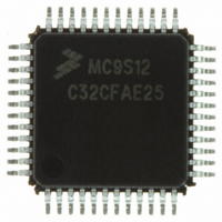
MC9S12C32CFAE25 Freescale Semiconductor, MC9S12C32CFAE25 Datasheet - Page 63

MC9S12C32CFAE25
Manufacturer Part Number
MC9S12C32CFAE25
Description
IC MCU 32K FLASH 25MHZ 48-LQFP
Manufacturer
Freescale Semiconductor
Series
HCS12r
Datasheets
1.MC9S12GC16MFUE.pdf
(690 pages)
2.MC9S12C96CFUER.pdf
(26 pages)
3.MC9S12C32CFAE25.pdf
(2 pages)
4.MC9S12C32CPBE25.pdf
(36 pages)
Specifications of MC9S12C32CFAE25
Core Processor
HCS12
Core Size
16-Bit
Speed
25MHz
Connectivity
CAN, EBI/EMI, SCI, SPI
Peripherals
POR, PWM, WDT
Number Of I /o
31
Program Memory Size
32KB (32K x 8)
Program Memory Type
FLASH
Ram Size
2K x 8
Voltage - Supply (vcc/vdd)
2.35 V ~ 5.5 V
Data Converters
A/D 8x10b
Oscillator Type
Internal
Operating Temperature
-40°C ~ 85°C
Package / Case
48-LQFP
Processor Series
S12C
Core
HCS12
Data Bus Width
16 bit
Data Ram Size
2 KB
Interface Type
CAN/SCI/SPI
Maximum Clock Frequency
25 MHz
Number Of Programmable I/os
31
Number Of Timers
8
Maximum Operating Temperature
+ 85 C
Mounting Style
SMD/SMT
3rd Party Development Tools
EWHCS12
Development Tools By Supplier
M68EVB912C32EE
Minimum Operating Temperature
- 40 C
On-chip Adc
8-ch x 10-bit
For Use With
CML12C32SLK - KIT STUDENT LEARNING 16BIT HCS12
Lead Free Status / RoHS Status
Lead free / RoHS Compliant
Eeprom Size
-
Lead Free Status / Rohs Status
Lead free / RoHS Compliant
Available stocks
Company
Part Number
Manufacturer
Quantity
Price
Company:
Part Number:
MC9S12C32CFAE25
Manufacturer:
FREESCAL
Quantity:
240
Company:
Part Number:
MC9S12C32CFAE25
Manufacturer:
Freescale Semiconductor
Quantity:
10 000
- MC9S12GC16MFUE PDF datasheet
- MC9S12C96CFUER PDF datasheet #2
- MC9S12C32CFAE25 PDF datasheet #3
- MC9S12C32CPBE25 PDF datasheet #4
- Current page: 63 of 690
- Download datasheet (4Mb)
1.7.2
The BDM section reference to alternate clock is equivalent to the oscillator clock.
1.7.3
In order to emulate the MC9S12GC or MC9S12C-Family / MC9S12GC-Family devices, external
addressing of a 128K memory map is required. This is provided in a 112 LQFP package version which
includes the 3 necessary extra external address bus signals via PortK[2:0]. This package version is for
emulation only and not provided as a general production package.
The reset state of DDRK is 0x0000, configuring the pins as inputs.
The reset state of PUPKE in the PUCR register is “1” enabling the internal Port K pullups.
In this reset state the pull-ups provide a defined state and prevent a floating input, thereby preventing
unnecessary current flow at the input stage.
To prevent unnecessary current flow in production package options, the states of DDRK and PUPKE
should not be changed by software.
Freescale Semiconductor
MC9S12GC128
MC9S12GC16
MC9S12GC32
MC9S12GC64
MC9S12GC96
MC9S12C128
MC9S12C32
MC9S12C64
MC9S12C96
Device
BDM Alternate Clock
Extended Address Range Emulation Implications
PAGE
3E
3C
3D
3E
3A
3B
3C
3D
3E
3A
3B
3C
3D
3E
3F
3F
3F
3F
38
39
3F
$00,$02,$04,$06,$08,$0A,$0C,$0E,$10,$12......$2C,$2E,$30,$32,$34,$36,$38,$3A,$3C,$3E
$01,$03,$05,$07,$09,$0B,$0D,$0F,$11,$13.....$2D,$2F,$31,$33,$35,$37,$39,$3B,$3D,$3F
Table 1-11. Device Specific Flash PAGE Mapping
MC9S12C-Family / MC9S12GC-Family
$01,$03,$05,$07,$09......$35,$37,$39,$3B,$3D,$3F
Rev 01.24
PAGE Visible with PPAGE Contents
$04,$0C,$14,$1C,$24,$2C,$34,$3C
$04,$0C,$14,$1C,$24,$2C,$34,$3C
$04,$0C,$14,$1C,$24,$2C,$34,$3C
Chapter 1 MC9S12C and MC9S12GC Device Overview (MC9S12C128)
$05,$0D,$15,$1D,$25,$2D,$35,$3D
$06,$0E,$16,$1E,$26,$2E,$36,$3E
$02,$0A,$12,$1A,$22,$2A,$32,$3A
$03,$0B,$13,$1B,$23,$2B,$33,$3B
$05,$0D,$15,$1D,$25,$2D,$35,$3D
$06,$0E,$16,$1E,$26,$2E,$36,$3E
$02,$0A,$12,$1A,$22,$2A,$32,$3A
$03,$0B,$13,$1B,$23,$2B,$33,$3B
$05,$0D,$15,$1D,$25,$2D,$35,$3D
$06,$0E,$16,$1E,$26,$2E,$36,$3E
$00,$08,$10,$18,$20,$28,$30,$38
$01,$09,$11,$19,$21,$29,$31,$39
$07,$0F,$17,$1F,$27,$2F,$37,$3F
$07,$0F,$17,$1F,$27,$2F,$37,$3F
$07,$0F,$17,$1F,$27,$2F,$37,$3F
63
Related parts for MC9S12C32CFAE25
Image
Part Number
Description
Manufacturer
Datasheet
Request
R
Part Number:
Description:
Manufacturer:
Freescale Semiconductor, Inc
Datasheet:
Part Number:
Description:
Manufacturer:
Freescale Semiconductor, Inc
Datasheet:
Part Number:
Description:
Manufacturer:
Freescale Semiconductor, Inc
Datasheet:
Part Number:
Description:
Manufacturer:
Freescale Semiconductor, Inc
Datasheet:
Part Number:
Description:
Manufacturer:
Freescale Semiconductor, Inc
Datasheet:
Part Number:
Description:
Manufacturer:
Freescale Semiconductor, Inc
Datasheet:
Part Number:
Description:
Manufacturer:
Freescale Semiconductor, Inc
Datasheet:
Part Number:
Description:
Manufacturer:
Freescale Semiconductor, Inc
Datasheet:
Part Number:
Description:
Manufacturer:
Freescale Semiconductor, Inc
Datasheet:
Part Number:
Description:
Manufacturer:
Freescale Semiconductor, Inc
Datasheet:
Part Number:
Description:
Manufacturer:
Freescale Semiconductor, Inc
Datasheet:
Part Number:
Description:
Manufacturer:
Freescale Semiconductor, Inc
Datasheet:
Part Number:
Description:
Manufacturer:
Freescale Semiconductor, Inc
Datasheet:
Part Number:
Description:
Manufacturer:
Freescale Semiconductor, Inc
Datasheet:
Part Number:
Description:
Manufacturer:
Freescale Semiconductor, Inc
Datasheet:


