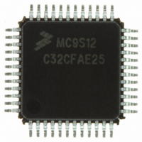
MC9S12C32CFAE25 Freescale Semiconductor, MC9S12C32CFAE25 Datasheet - Page 55

MC9S12C32CFAE25
Manufacturer Part Number
MC9S12C32CFAE25
Description
IC MCU 32K FLASH 25MHZ 48-LQFP
Manufacturer
Freescale Semiconductor
Series
HCS12r
Datasheets
1.MC9S12GC16MFUE.pdf
(690 pages)
2.MC9S12C96CFUER.pdf
(26 pages)
3.MC9S12C32CFAE25.pdf
(2 pages)
4.MC9S12C32CPBE25.pdf
(36 pages)
Specifications of MC9S12C32CFAE25
Core Processor
HCS12
Core Size
16-Bit
Speed
25MHz
Connectivity
CAN, EBI/EMI, SCI, SPI
Peripherals
POR, PWM, WDT
Number Of I /o
31
Program Memory Size
32KB (32K x 8)
Program Memory Type
FLASH
Ram Size
2K x 8
Voltage - Supply (vcc/vdd)
2.35 V ~ 5.5 V
Data Converters
A/D 8x10b
Oscillator Type
Internal
Operating Temperature
-40°C ~ 85°C
Package / Case
48-LQFP
Processor Series
S12C
Core
HCS12
Data Bus Width
16 bit
Data Ram Size
2 KB
Interface Type
CAN/SCI/SPI
Maximum Clock Frequency
25 MHz
Number Of Programmable I/os
31
Number Of Timers
8
Maximum Operating Temperature
+ 85 C
Mounting Style
SMD/SMT
3rd Party Development Tools
EWHCS12
Development Tools By Supplier
M68EVB912C32EE
Minimum Operating Temperature
- 40 C
On-chip Adc
8-ch x 10-bit
For Use With
CML12C32SLK - KIT STUDENT LEARNING 16BIT HCS12
Lead Free Status / RoHS Status
Lead free / RoHS Compliant
Eeprom Size
-
Lead Free Status / Rohs Status
Lead free / RoHS Compliant
Available stocks
Company
Part Number
Manufacturer
Quantity
Price
Company:
Part Number:
MC9S12C32CFAE25
Manufacturer:
FREESCAL
Quantity:
240
Company:
Part Number:
MC9S12C32CFAE25
Manufacturer:
Freescale Semiconductor
Quantity:
10 000
- MC9S12GC16MFUE PDF datasheet
- MC9S12C96CFUER PDF datasheet #2
- MC9S12C32CFAE25 PDF datasheet #3
- MC9S12C32CPBE25 PDF datasheet #4
- Current page: 55 of 690
- Download datasheet (4Mb)
1.3.4.27
PS3 and PS2 are general purpose input or output pins. These pins are not available in the 48- / 52-pin
package versions.
1.3.4.28
PS1 is a general purpose input or output pin and the transmit pin, TXD, of serial communication interface
(SCI).
1.3.4.29
PS0 is a general purpose input or output pin and the receive pin, RXD, of serial communication interface
(SCI).
1.3.4.30
PT7–PT5 are general purpose input or output pins. They can also be configured as the timer system input
capture or output compare pins IOC7-IOC5.
1.3.4.31
PT4–PT0 are general purpose input or output pins. They can also be configured as the timer system input
capture or output compare pins IOC[n] or as the PWM outputs PW[n].
1.3.5
1.3.5.1
External power and ground for I/O drivers. Bypass requirements depend on how heavily the MCU pins are
loaded.
1.3.5.2
External power and ground for the internal voltage regulator. Connecting V
internal voltage regulator.
1.3.5.3
Power is supplied to the MCU through V
regulator. There is no static load on those pins allowed. The internal voltage regulator is turned off, if V
is tied to ground.
Freescale Semiconductor
Power Supply Pins
PS[3:2] — Port S I/O Pins [3:2]
PS1 / TXD — Port S I/O Pin 1
PS0 / RXD — Port S I/O Pin 0
PT[7:5] / IOC[7:5] — Port T I/O Pins [7:5]
PT[4:0] / IOC[4:0] / PW[4:0]— Port T I/O Pins [4:0]
V
V
Voltage Regulator
V
DDX
DDR
DD1
, V
,V
, V
SSX
DD2
SSR
, V
— Power and Ground Pins for I/O Drivers
— Power and Ground Pins for I/O Drivers and for Internal
SS1
, V
MC9S12C-Family / MC9S12GC-Family
SS2
DD
— Internal Logic Power Pins
and V
Rev 01.24
SS
Chapter 1 MC9S12C and MC9S12GC Device Overview (MC9S12C128)
. This 2.5V supply is derived from the internal voltage
DDR
to ground disables the
DDR
55
Related parts for MC9S12C32CFAE25
Image
Part Number
Description
Manufacturer
Datasheet
Request
R
Part Number:
Description:
Manufacturer:
Freescale Semiconductor, Inc
Datasheet:
Part Number:
Description:
Manufacturer:
Freescale Semiconductor, Inc
Datasheet:
Part Number:
Description:
Manufacturer:
Freescale Semiconductor, Inc
Datasheet:
Part Number:
Description:
Manufacturer:
Freescale Semiconductor, Inc
Datasheet:
Part Number:
Description:
Manufacturer:
Freescale Semiconductor, Inc
Datasheet:
Part Number:
Description:
Manufacturer:
Freescale Semiconductor, Inc
Datasheet:
Part Number:
Description:
Manufacturer:
Freescale Semiconductor, Inc
Datasheet:
Part Number:
Description:
Manufacturer:
Freescale Semiconductor, Inc
Datasheet:
Part Number:
Description:
Manufacturer:
Freescale Semiconductor, Inc
Datasheet:
Part Number:
Description:
Manufacturer:
Freescale Semiconductor, Inc
Datasheet:
Part Number:
Description:
Manufacturer:
Freescale Semiconductor, Inc
Datasheet:
Part Number:
Description:
Manufacturer:
Freescale Semiconductor, Inc
Datasheet:
Part Number:
Description:
Manufacturer:
Freescale Semiconductor, Inc
Datasheet:
Part Number:
Description:
Manufacturer:
Freescale Semiconductor, Inc
Datasheet:
Part Number:
Description:
Manufacturer:
Freescale Semiconductor, Inc
Datasheet:


