MC9S12C32CFAE25 Freescale Semiconductor, MC9S12C32CFAE25 Datasheet - Page 82
MC9S12C32CFAE25
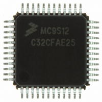
Manufacturer Part Number
MC9S12C32CFAE25
Description
IC MCU 32K FLASH 25MHZ 48-LQFP
Manufacturer
Freescale Semiconductor
Series
HCS12r
Datasheets
1.MC9S12GC16MFUE.pdf
(690 pages)
2.MC9S12C96CFUER.pdf
(26 pages)
3.MC9S12C32CFAE25.pdf
(2 pages)
4.MC9S12C32CPBE25.pdf
(36 pages)
Specifications of MC9S12C32CFAE25
Core Processor
HCS12
Core Size
16-Bit
Speed
25MHz
Connectivity
CAN, EBI/EMI, SCI, SPI
Peripherals
POR, PWM, WDT
Number Of I /o
31
Program Memory Size
32KB (32K x 8)
Program Memory Type
FLASH
Ram Size
2K x 8
Voltage - Supply (vcc/vdd)
2.35 V ~ 5.5 V
Data Converters
A/D 8x10b
Oscillator Type
Internal
Operating Temperature
-40°C ~ 85°C
Package / Case
48-LQFP
Processor Series
S12C
Core
HCS12
Data Bus Width
16 bit
Data Ram Size
2 KB
Interface Type
CAN/SCI/SPI
Maximum Clock Frequency
25 MHz
Number Of Programmable I/os
31
Number Of Timers
8
Maximum Operating Temperature
+ 85 C
Mounting Style
SMD/SMT
3rd Party Development Tools
EWHCS12
Development Tools By Supplier
M68EVB912C32EE
Minimum Operating Temperature
- 40 C
On-chip Adc
8-ch x 10-bit
For Use With
CML12C32SLK - KIT STUDENT LEARNING 16BIT HCS12
Lead Free Status / RoHS Status
Lead free / RoHS Compliant
Eeprom Size
-
Lead Free Status / Rohs Status
Lead free / RoHS Compliant
Available stocks
Company
Part Number
Manufacturer
Quantity
Price
Company:

Part Number:
MC9S12C32CFAE25
Manufacturer:
FREESCAL
Quantity:
240
Company:
Part Number:
MC9S12C32CFAE25
Manufacturer:
Freescale Semiconductor
Quantity:
10 000


Chapter 2 Port Integration Module (PIM9C32) Block Description
2.3.2.1.2
Read: Anytime.
Write: Never, writes to this register have no effect.
2.3.2.1.3
Read: Anytime.
Write: Anytime.
82
Module Base + 0x0001
Module Base + 0x0002
DDRT[7:0]
PTIT[7:0]
Reset
Reset
Field
Field
7–0
7–0
W
W
R
R
DDRT7
PTIT7
Port T Input Register — This register always reads back the status of the associated pins. This can also be
used to detect overload or short circuit conditions on output pins.
Data Direction Port T — This register configures each port T pin as either input or output.
The standard TIM / PWM modules forces the I/O state to be an output for each standard TIM / PWM module port
associated with an enabled output compare. In these cases the data direction bits will not change.
The DDRT bits revert to controlling the I/O direction of a pin when the associated timer output compare is
disabled.
The timer input capture always monitors the state of the pin.
0 Associated pin is configured as input.
1 Associated pin is configured as output.
Note: Due to internal synchronization circuits, it can take up to 2 bus cycles until the correct value is read on PTT
—
0
7
7
Port T Input Register (PTIT)
Port T Data Direction Register (DDRT)
or PTIT registers, when changing the DDRT register.
= Unimplemented or Reserved
DDRT6
PTIT6
—
0
6
6
Figure 2-5. Port T Data Direction Register (DDRT)
Figure 2-4. Port T Input Register (PTIT)
Table 2-5. DDRT Field Descriptions
DDRT5
Table 2-4. PTIT Field Descriptions
PTIT5
MC9S12C-Family / MC9S12GC-Family
—
0
5
5
DDRT4
PTIT4
Rev 01.24
—
0
4
4
Description
Description
DDRT3
PTIT3
—
0
3
3
DDRT2
PTIT2
—
0
2
2
DDRT1
Freescale Semiconductor
PTIT1
—
0
1
1
DDRT0
PTIT0
—
0
0
0
Related parts for MC9S12C32CFAE25
Image
Part Number
Description
Manufacturer
Datasheet
Request
R

Part Number:
Description:
Manufacturer:
Freescale Semiconductor, Inc
Datasheet:
Part Number:
Description:
Manufacturer:
Freescale Semiconductor, Inc
Datasheet:
Part Number:
Description:
Manufacturer:
Freescale Semiconductor, Inc
Datasheet:
Part Number:
Description:
Manufacturer:
Freescale Semiconductor, Inc
Datasheet:
Part Number:
Description:
Manufacturer:
Freescale Semiconductor, Inc
Datasheet:
Part Number:
Description:
Manufacturer:
Freescale Semiconductor, Inc
Datasheet:
Part Number:
Description:
Manufacturer:
Freescale Semiconductor, Inc
Datasheet:
Part Number:
Description:
Manufacturer:
Freescale Semiconductor, Inc
Datasheet:
Part Number:
Description:
Manufacturer:
Freescale Semiconductor, Inc
Datasheet:
Part Number:
Description:
Manufacturer:
Freescale Semiconductor, Inc
Datasheet:
Part Number:
Description:
Manufacturer:
Freescale Semiconductor, Inc
Datasheet:
Part Number:
Description:
Manufacturer:
Freescale Semiconductor, Inc
Datasheet:
Part Number:
Description:
Manufacturer:
Freescale Semiconductor, Inc
Datasheet:
Part Number:
Description:
Manufacturer:
Freescale Semiconductor, Inc
Datasheet:
Part Number:
Description:
Manufacturer:
Freescale Semiconductor, Inc
Datasheet: