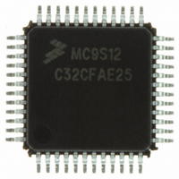
MC9S12C32CFAE25 Freescale Semiconductor, MC9S12C32CFAE25 Datasheet - Page 143

MC9S12C32CFAE25
Manufacturer Part Number
MC9S12C32CFAE25
Description
IC MCU 32K FLASH 25MHZ 48-LQFP
Manufacturer
Freescale Semiconductor
Series
HCS12r
Datasheets
1.MC9S12GC16MFUE.pdf
(690 pages)
2.MC9S12C96CFUER.pdf
(26 pages)
3.MC9S12C32CFAE25.pdf
(2 pages)
4.MC9S12C32CPBE25.pdf
(36 pages)
Specifications of MC9S12C32CFAE25
Core Processor
HCS12
Core Size
16-Bit
Speed
25MHz
Connectivity
CAN, EBI/EMI, SCI, SPI
Peripherals
POR, PWM, WDT
Number Of I /o
31
Program Memory Size
32KB (32K x 8)
Program Memory Type
FLASH
Ram Size
2K x 8
Voltage - Supply (vcc/vdd)
2.35 V ~ 5.5 V
Data Converters
A/D 8x10b
Oscillator Type
Internal
Operating Temperature
-40°C ~ 85°C
Package / Case
48-LQFP
Processor Series
S12C
Core
HCS12
Data Bus Width
16 bit
Data Ram Size
2 KB
Interface Type
CAN/SCI/SPI
Maximum Clock Frequency
25 MHz
Number Of Programmable I/os
31
Number Of Timers
8
Maximum Operating Temperature
+ 85 C
Mounting Style
SMD/SMT
3rd Party Development Tools
EWHCS12
Development Tools By Supplier
M68EVB912C32EE
Minimum Operating Temperature
- 40 C
On-chip Adc
8-ch x 10-bit
For Use With
CML12C32SLK - KIT STUDENT LEARNING 16BIT HCS12
Lead Free Status / RoHS Status
Lead free / RoHS Compliant
Eeprom Size
-
Lead Free Status / Rohs Status
Lead free / RoHS Compliant
Available stocks
Company
Part Number
Manufacturer
Quantity
Price
Company:
Part Number:
MC9S12C32CFAE25
Manufacturer:
FREESCAL
Quantity:
240
Company:
Part Number:
MC9S12C32CFAE25
Manufacturer:
Freescale Semiconductor
Quantity:
10 000
- MC9S12GC16MFUE PDF datasheet
- MC9S12C96CFUER PDF datasheet #2
- MC9S12C32CFAE25 PDF datasheet #3
- MC9S12C32CPBE25 PDF datasheet #4
- Current page: 143 of 690
- Download datasheet (4Mb)
4.3.2.9
Read: Anytime (provided this register is in the map).
Write: Each bit has specific write conditions. Please refer to the descriptions of each bit on the following
pages.
The MODE register is used to establish the operating mode and other miscellaneous functions (i.e.,
internal visibility and emulation of port E and K).
In special peripheral mode, this register is not accessible but it is reset as shown to system configuration
features. Changes to bits in the MODE register are delayed one cycle after the write.
This register is not in the on-chip memory map in expanded and special peripheral modes. Therefore, these
accesses will be echoed externally.
Freescale Semiconductor
Module Base + 0x000B
Starting address location affected by INITRG register setting.
Normal Expanded Wide
Emulation Expanded
Emulation Expanded
Special Single Chip
Normal Single Chip
Normal Expanded
Special Test
Peripheral
Mode Register (MODE)
Narrow
Narrow
Reset
Wide
W
R
MODC
0
0
0
0
1
1
1
1
7
= Unimplemented or Reserved
MODB
Figure 4-13. Mode Register (MODE)
MC9S12C-Family / MC9S12GC-Family
0
0
1
1
0
0
1
1
6
MODA
0
1
0
1
0
1
0
1
5
Rev 01.24
4
0
0
0
0
0
0
0
0
0
Chapter 4 Multiplexed External Bus Interface (MEBIV3)
IVIS
0
1
1
1
0
0
0
0
3
0
0
0
0
0
0
0
0
0
2
EMK
0
1
0
1
0
0
0
0
1
EME
0
1
0
1
0
0
0
0
0
143
Related parts for MC9S12C32CFAE25
Image
Part Number
Description
Manufacturer
Datasheet
Request
R
Part Number:
Description:
Manufacturer:
Freescale Semiconductor, Inc
Datasheet:
Part Number:
Description:
Manufacturer:
Freescale Semiconductor, Inc
Datasheet:
Part Number:
Description:
Manufacturer:
Freescale Semiconductor, Inc
Datasheet:
Part Number:
Description:
Manufacturer:
Freescale Semiconductor, Inc
Datasheet:
Part Number:
Description:
Manufacturer:
Freescale Semiconductor, Inc
Datasheet:
Part Number:
Description:
Manufacturer:
Freescale Semiconductor, Inc
Datasheet:
Part Number:
Description:
Manufacturer:
Freescale Semiconductor, Inc
Datasheet:
Part Number:
Description:
Manufacturer:
Freescale Semiconductor, Inc
Datasheet:
Part Number:
Description:
Manufacturer:
Freescale Semiconductor, Inc
Datasheet:
Part Number:
Description:
Manufacturer:
Freescale Semiconductor, Inc
Datasheet:
Part Number:
Description:
Manufacturer:
Freescale Semiconductor, Inc
Datasheet:
Part Number:
Description:
Manufacturer:
Freescale Semiconductor, Inc
Datasheet:
Part Number:
Description:
Manufacturer:
Freescale Semiconductor, Inc
Datasheet:
Part Number:
Description:
Manufacturer:
Freescale Semiconductor, Inc
Datasheet:
Part Number:
Description:
Manufacturer:
Freescale Semiconductor, Inc
Datasheet:


