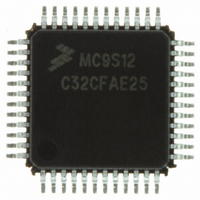
MC9S12C32CFAE25 Freescale Semiconductor, MC9S12C32CFAE25 Datasheet - Page 298
MC9S12C32CFAE25
Manufacturer Part Number
MC9S12C32CFAE25
Description
IC MCU 32K FLASH 25MHZ 48-LQFP
Manufacturer
Freescale Semiconductor
Series
HCS12r
Datasheets
1.MC9S12GC16MFUE.pdf
(690 pages)
2.MC9S12C96CFUER.pdf
(26 pages)
3.MC9S12C32CFAE25.pdf
(2 pages)
4.MC9S12C32CPBE25.pdf
(36 pages)
Specifications of MC9S12C32CFAE25
Core Processor
HCS12
Core Size
16-Bit
Speed
25MHz
Connectivity
CAN, EBI/EMI, SCI, SPI
Peripherals
POR, PWM, WDT
Number Of I /o
31
Program Memory Size
32KB (32K x 8)
Program Memory Type
FLASH
Ram Size
2K x 8
Voltage - Supply (vcc/vdd)
2.35 V ~ 5.5 V
Data Converters
A/D 8x10b
Oscillator Type
Internal
Operating Temperature
-40°C ~ 85°C
Package / Case
48-LQFP
Processor Series
S12C
Core
HCS12
Data Bus Width
16 bit
Data Ram Size
2 KB
Interface Type
CAN/SCI/SPI
Maximum Clock Frequency
25 MHz
Number Of Programmable I/os
31
Number Of Timers
8
Maximum Operating Temperature
+ 85 C
Mounting Style
SMD/SMT
3rd Party Development Tools
EWHCS12
Development Tools By Supplier
M68EVB912C32EE
Minimum Operating Temperature
- 40 C
On-chip Adc
8-ch x 10-bit
For Use With
CML12C32SLK - KIT STUDENT LEARNING 16BIT HCS12
Lead Free Status / RoHS Status
Lead free / RoHS Compliant
Eeprom Size
-
Lead Free Status / Rohs Status
Lead free / RoHS Compliant
Available stocks
Company
Part Number
Manufacturer
Quantity
Price
Company:

Part Number:
MC9S12C32CFAE25
Manufacturer:
FREESCAL
Quantity:
240
Company:
Part Number:
MC9S12C32CFAE25
Manufacturer:
Freescale Semiconductor
Quantity:
10 000


Chapter 10 Freescale’s Scalable Controller Area Network (S12MSCANV2)
10.3.2.4
The CANBTR1 register configures various CAN bus timing parameters of the MSCAN module.
Read: Anytime
Write: Anytime in initialization mode (INITRQ = 1 and INITAK = 1)
1. In this case, PHASE_SEG1 must be at least 2 time quanta (Tq).
298
Module Base + 0x0003
TSEG2[2:0]
TSEG1[3:0]
SAMP
Field
6:4
3:0
7
Reset:
W
R
Sampling — This bit determines the number of CAN bus samples taken per bit time.
0 One sample per bit.
1 Three samples per bit
If SAMP = 0, the resulting bit value is equal to the value of the single bit positioned at the sample point. If
SAMP = 1, the resulting bit value is determined by using majority rule on the three total samples. For higher bit
rates, it is recommended that only one sample is taken per bit time (SAMP = 0).
Time Segment 2 — Time segments within the bit time fix the number of clock cycles per bit time and the location
of the sample point (see
Table
Time Segment 1 — Time segments within the bit time fix the number of clock cycles per bit time and the location
of the sample point (see
Table
MSCAN Bus Timing Register 1 (CANBTR1)
SAMP
1. This setting is not valid. Please refer to
0
7
10-7.
10-8.
TSEG22
0
0
1
1
:
Figure 10-7. MSCAN Bus Timing Register 1 (CANBTR1)
TSEG22
Table 10-6. CANBTR1 Register Field Descriptions
6
0
(1)
Figure
Figure
.
TSEG21
Table 10-7. Time Segment 2 Values
MC9S12C-Family / MC9S12GC-Family
TSEG21
0
0
1
1
:
10-43). Time segment 2 (TSEG2) values are programmable as shown in
10-43). Time segment 1 (TSEG1) values are programmable as shown in
0
5
Rev 01.24
TSEG20
TSEG20
Table 10-34
4
0
0
1
0
1
:
Description
TSEG13
for valid settings.
0
3
1 Tq clock cycle
Time Segment 2
2 Tq clock cycles
7 Tq clock cycles
8 Tq clock cycles
TSEG12
:
2
0
(1)
TSEG11
Freescale Semiconductor
0
1
TSEG10
0
0
Related parts for MC9S12C32CFAE25
Image
Part Number
Description
Manufacturer
Datasheet
Request
R

Part Number:
Description:
Manufacturer:
Freescale Semiconductor, Inc
Datasheet:
Part Number:
Description:
Manufacturer:
Freescale Semiconductor, Inc
Datasheet:
Part Number:
Description:
Manufacturer:
Freescale Semiconductor, Inc
Datasheet:
Part Number:
Description:
Manufacturer:
Freescale Semiconductor, Inc
Datasheet:
Part Number:
Description:
Manufacturer:
Freescale Semiconductor, Inc
Datasheet:
Part Number:
Description:
Manufacturer:
Freescale Semiconductor, Inc
Datasheet:
Part Number:
Description:
Manufacturer:
Freescale Semiconductor, Inc
Datasheet:
Part Number:
Description:
Manufacturer:
Freescale Semiconductor, Inc
Datasheet:
Part Number:
Description:
Manufacturer:
Freescale Semiconductor, Inc
Datasheet:
Part Number:
Description:
Manufacturer:
Freescale Semiconductor, Inc
Datasheet:
Part Number:
Description:
Manufacturer:
Freescale Semiconductor, Inc
Datasheet:
Part Number:
Description:
Manufacturer:
Freescale Semiconductor, Inc
Datasheet:
Part Number:
Description:
Manufacturer:
Freescale Semiconductor, Inc
Datasheet:
Part Number:
Description:
Manufacturer:
Freescale Semiconductor, Inc
Datasheet:
Part Number:
Description:
Manufacturer:
Freescale Semiconductor, Inc
Datasheet: