AT91SAM9M10-CU Atmel, AT91SAM9M10-CU Datasheet - Page 383
AT91SAM9M10-CU
Manufacturer Part Number
AT91SAM9M10-CU
Description
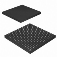
IC MCU 16/32BIT ARM9 324TFBGA
Manufacturer
Atmel
Series
AT91SAMr
Specifications of AT91SAM9M10-CU
Core Processor
ARM9
Core Size
16/32-Bit
Speed
400MHz
Connectivity
EBI/EMI, Ethernet, I²C, SPI, SSC, UART/USART, USB
Peripherals
AC'97, DMA, LCD, POR, PWM, WDT
Number Of I /o
160
Program Memory Size
64KB (64K x 8)
Program Memory Type
ROM
Ram Size
128K x 8
Voltage - Supply (vcc/vdd)
0.9 V ~ 1.1 V
Data Converters
A/D 8x10b
Oscillator Type
Internal
Operating Temperature
-40°C ~ 85°C
Package / Case
324-TFBGA
Processor Series
AT91SAMx
Core
ARM926EJ-S
Data Bus Width
32 bit
Data Ram Size
32 KB
Interface Type
2-Wire, SPI, USART
Maximum Clock Frequency
133 MHz
Number Of Programmable I/os
5
Number Of Timers
2 x 16 bit
Operating Supply Voltage
1.65 V to 3.6 V
Maximum Operating Temperature
+ 85 C
Mounting Style
SMD/SMT
3rd Party Development Tools
JTRACE-ARM-2M, MDK-ARM, RL-ARM, ULINK2
Development Tools By Supplier
AT91SAM-ICE, AT91-ISP, AT91SAM9M10-G45-EK
Controller Family/series
AT91
No. Of I/o's
160
Ram Memory Size
64KB
Cpu Speed
400MHz
No. Of Timers
2
Rohs Compliant
Yes
Cpu Family
AT91
Device Core
ARM926EJ-S
Device Core Size
32b
Frequency (max)
400MHz
Total Internal Ram Size
64KB
# I/os (max)
160
Number Of Timers - General Purpose
7
Operating Supply Voltage (typ)
1.8/2.5/3.3V
Operating Supply Voltage (max)
1.1/1.95/3.6V
Operating Supply Voltage (min)
0.9/1.65/1.8/3V
On-chip Adc
8-chx10-bit
Instruction Set Architecture
RISC
Operating Temp Range
-40C to 85C
Operating Temperature Classification
Industrial
Mounting
Surface Mount
Pin Count
324
Package Type
TFBGA
Lead Free Status / RoHS Status
Lead free / RoHS Compliant
Eeprom Size
-
Lead Free Status / Rohs Status
Lead free / RoHS Compliant
Available stocks
Company
Part Number
Manufacturer
Quantity
Price
Company:

Part Number:
AT91SAM9M10-CU
Manufacturer:
Atmel
Quantity:
996


27.8.4.5
6355B–ATARM–21-Jun-10
Fast Forcing
Note:
Another way to handle the fast interrupt is to map the interrupt service routine at the address of
the ARM vector 0x1C. This method does not use the vectoring, so that reading AIC_FVR must
be performed at the very beginning of the handler operation. However, this method saves the
execution of a branch instruction.
The Fast Forcing feature of the advanced interrupt controller provides redirection of any normal
Interrupt source on the fast interrupt controller.
Fast Forcing is enabled or disabled by writing to the Fast Forcing Enable Register (AIC_FFER)
and the Fast Forcing Disable Register (AIC_FFDR). Writing to these registers results in an
update of the Fast Forcing Status Register (AIC_FFSR) that controls the feature for each inter-
nal or external interrupt source.
When Fast Forcing is disabled, the interrupt sources are handled as described in the previous
pages.
When Fast Forcing is enabled, the edge/level programming and, in certain cases, edge detec-
tion of the interrupt source is still active but the source cannot trigger a normal interrupt to the
processor and is not seen by the priority handler.
If the interrupt source is programmed in level-sensitive mode and an active level is sampled,
Fast Forcing results in the assertion of the nFIQ line to the core.
If the interrupt source is programmed in edge-triggered mode and an active edge is detected,
Fast Forcing results in the assertion of the nFIQ line to the core.
The Fast Forcing feature does not affect the Source 0 pending bit in the Interrupt Pending Reg-
ister (AIC_IPR).
2. The ARM core enters FIQ mode.
3. When the instruction loaded at address 0x1C is executed, the program counter is
4. The previous step enables branching to the corresponding interrupt service routine. It is
5. The Interrupt Handler can then proceed as required. It is not necessary to save regis-
6. Finally, the Link Register R14_fiq is restored into the PC after decrementing it by four
the following cycle, during fetch at address 0x20, the ARM core adjusts R14_fiq, decre-
menting it by four.
loaded with the value read in AIC_FVR. Reading the AIC_FVR has effect of automati-
cally clearing the fast interrupt, if it has been programmed to be edge triggered. In this
case only, it de-asserts the nFIQ line on the processor.
not necessary to save the link register R14_fiq and SPSR_fiq if nested fast interrupts
are not needed.
ters R8 to R13 because FIQ mode has its own dedicated registers and the user R8 to
R13 are banked. The other registers, R0 to R7, must be saved before being used, and
restored at the end (before the next step). Note that if the fast interrupt is programmed
to be level sensitive, the source of the interrupt must be cleared during this phase in
order to de-assert the interrupt source 0.
(with instruction SUB PC, LR, #4 for example). This has the effect of returning from
the interrupt to whatever was being executed before, loading the CPSR with the SPSR
and masking or unmasking the fast interrupt depending on the state saved in the
SPSR.
The “F” bit in SPSR is significant. If it is set, it indicates that the ARM core was just about to mask
FIQ interrupts when the mask instruction was interrupted. Hence when the SPSR is restored, the
interrupted instruction is completed (FIQ is masked).
AT91SAM9M10
383
Related parts for AT91SAM9M10-CU
Image
Part Number
Description
Manufacturer
Datasheet
Request
R

Part Number:
Description:
MCU, MPU & DSP Development Tools KICKSTART KIT FOR AT91SAM9 PLUS
Manufacturer:
IAR Systems

Part Number:
Description:
DEV KIT FOR AVR/AVR32
Manufacturer:
Atmel
Datasheet:

Part Number:
Description:
INTERVAL AND WIPE/WASH WIPER CONTROL IC WITH DELAY
Manufacturer:
ATMEL Corporation
Datasheet:
Part Number:
Description:
Low-Voltage Voice-Switched IC for Hands-Free Operation
Manufacturer:
ATMEL Corporation
Datasheet:
Part Number:
Description:
MONOLITHIC INTEGRATED FEATUREPHONE CIRCUIT
Manufacturer:
ATMEL Corporation
Datasheet:
Part Number:
Description:
AM-FM Receiver IC U4255BM-M
Manufacturer:
ATMEL Corporation
Datasheet:
Part Number:
Description:
Monolithic Integrated Feature Phone Circuit
Manufacturer:
ATMEL Corporation
Datasheet:
Part Number:
Description:
Multistandard Video-IF and Quasi Parallel Sound Processing
Manufacturer:
ATMEL Corporation
Datasheet:
Part Number:
Description:
High-performance EE PLD
Manufacturer:
ATMEL Corporation
Datasheet:
Part Number:
Description:
8-bit Flash Microcontroller
Manufacturer:
ATMEL Corporation
Datasheet:
Part Number:
Description:
2-Wire Serial EEPROM
Manufacturer:
ATMEL Corporation
Datasheet: