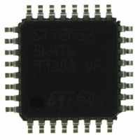
ST72F325K4T6 STMicroelectronics, ST72F325K4T6 Datasheet - Page 95

ST72F325K4T6
Manufacturer Part Number
ST72F325K4T6
Description
MCU 8BIT 16KB FLASH/ROM 32-LQFP
Manufacturer
STMicroelectronics
Series
ST7r
Datasheet
1.ST72F325K6T6.pdf
(197 pages)
Specifications of ST72F325K4T6
Core Processor
ST7
Core Size
8-Bit
Speed
8MHz
Connectivity
I²C, SCI, SPI
Peripherals
LVD, POR, PWM, WDT
Number Of I /o
24
Program Memory Size
16KB (16K x 8)
Program Memory Type
FLASH
Ram Size
512 x 8
Voltage - Supply (vcc/vdd)
3.8 V ~ 5.5 V
Data Converters
A/D 16x10b
Oscillator Type
Internal
Operating Temperature
-40°C ~ 85°C
Package / Case
32-LQFP
Processor Series
ST72F3x
Core
ST7
Data Bus Width
8 bit
Data Ram Size
512 B
Interface Type
I2C, SCI, SPI
Maximum Clock Frequency
8 MHz
Number Of Programmable I/os
48
Number Of Timers
2
Maximum Operating Temperature
+ 85 C
Mounting Style
SMD/SMT
Development Tools By Supplier
ST7232X-EVAL, ST7232X-SK/RAIS, ST72325-D/RAIS, ST7MDT20-DVP3, ST7MDT20J-EMU3, ST7MDT20M-EMU3, STX-RLINK
Minimum Operating Temperature
- 40 C
On-chip Adc
10 bit, 16 Channel
For Use With
497-5046 - KIT TOOL FOR ST7/UPSD/STR7 MCU
Lead Free Status / RoHS Status
Lead free / RoHS Compliant
Eeprom Size
-
Lead Free Status / Rohs Status
Details
Other names
497-5605
Available stocks
Company
Part Number
Manufacturer
Quantity
Price
Company:
Part Number:
ST72F325K4T6
Manufacturer:
ST
Quantity:
151
Company:
Part Number:
ST72F325K4T6
Manufacturer:
STMicroelectronics
Quantity:
10 000
Part Number:
ST72F325K4T6
Manufacturer:
ST
Quantity:
20 000
Company:
Part Number:
ST72F325K4T6TR
Manufacturer:
STMicroelectronics
Quantity:
10 000
SERIAL PERIPHERAL INTERFACE (Cont’d)
10.5.3.3 Master Mode Operation
In master mode, the serial clock is output on the
SCK pin. The clock frequency, polarity and phase
are configured by software (refer to the description
of the SPICSR register).
Note: The idle state of SCK must correspond to
the polarity selected in the SPICSR register (by
pulling up SCK if CPOL=1 or pulling down SCK if
CPOL=0).
To operate the SPI in master mode, perform the
following steps in order (if the SPICSR register is
not written first, the SPICR register setting
(MSTR bit) may be not taken into account):
1. Write to the SPICR register:
2. Write to the SPICSR register:
3. Write to the SPICR register:
The transmit sequence begins when software
writes a byte in the SPIDR register.
10.5.3.4 Master Mode Transmit Sequence
When software writes to the SPIDR register, the
data byte is loaded into the 8-bit shift register and
then shifted out serially to the MOSI pin most sig-
nificant bit first.
When data transfer is complete:
Clearing the SPIF bit is performed by the following
software sequence:
1. An access to the SPICSR register while the
2. A read to the SPIDR register.
– Select the clock frequency by configuring the
– Select the clock polarity and clock phase by
– Either set the SSM bit and set the SSI bit or
– Set the MSTR and SPE bits
– The SPIF bit is set by hardware
– An interrupt request is generated if the SPIE
SPIF bit is set
SPR[2:0] bits.
configuring the CPOL and CPHA bits.
60
Note: The slave must have the same CPOL
and CPHA settings as the master.
clear the SSM bit and tie the SS pin high for
the complete byte transmit sequence.
Note: MSTR and SPE bits remain set only if
SS is high).
bit is set and the interrupt mask in the CCR
register is cleared.
shows the four possible configurations.
Figure
Note: While the SPIF bit is set, all writes to the
SPIDR register are inhibited until the SPICSR reg-
ister is read.
10.5.3.5 Slave Mode Operation
In slave mode, the serial clock is received on the
SCK pin from the master device.
To operate the SPI in slave mode:
1. Write to the SPICSR register to perform the fol-
2. Write to the SPICR register to clear the MSTR
10.5.3.6 Slave Mode Transmit Sequence
When software writes to the SPIDR register, the
data byte is loaded into the 8-bit shift register and
then shifted out serially to the MISO pin most sig-
nificant bit first.
The transmit sequence begins when the slave de-
vice receives the clock signal and the most signifi-
cant bit of the data on its MOSI pin.
When data transfer is complete:
Clearing the SPIF bit is performed by the following
software sequence:
1. An access to the SPICSR register while the
2. A write or a read to the SPIDR register.
Notes: While the SPIF bit is set, all writes to the
SPIDR register are inhibited until the SPICSR reg-
ister is read.
The SPIF bit can be cleared during a second
transmission; however, it must be cleared before
the second SPIF bit in order to prevent an Overrun
condition (see
lowing actions:
– Select the clock polarity and clock phase by
– Manage the SS pin as described in
bit and set the SPE bit to enable the SPI I/O
functions.
– The SPIF bit is set by hardware
– An interrupt request is generated if SPIE bit is
SPIF bit is set.
configuring the CPOL and CPHA bits (see
Figure
Note: The slave must have the same CPOL
and CPHA settings as the master.
10.5.3.2
be held low continuously. If CPHA=0 SS must
be held low during byte transmission and
pulled up between each byte to let the slave
write in the shift register.
set and interrupt mask in the CCR register is
cleared.
60).
and
Section
Figure
10.5.5.2).
58. If CPHA=1 SS must
ST72325xx
Section
95/197


