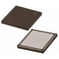
PIC18F65K22-I/MRRSL Microchip Technology, PIC18F65K22-I/MRRSL Datasheet - Page 125

PIC18F65K22-I/MRRSL
Manufacturer Part Number
PIC18F65K22-I/MRRSL
Description
MCU PIC 32K FLASH MEM XLP 64QFN
Manufacturer
Microchip Technology
Series
PIC® XLP™ 18Fr
Datasheets
1.PIC16F722-ISS.pdf
(8 pages)
2.PIC18F65K22T-IPTRSL.pdf
(548 pages)
3.PIC18F65K22T-IPTRSL.pdf
(10 pages)
Specifications of PIC18F65K22-I/MRRSL
Core Size
8-Bit
Program Memory Size
32KB (16K x 16)
Core Processor
PIC
Speed
64MHz
Connectivity
I²C, LIN, SPI, UART/USART
Peripherals
Brown-out Detect/Reset, LVD, POR, PWM, WDT
Number Of I /o
53
Program Memory Type
FLASH
Eeprom Size
1K x 8
Ram Size
2K x 8
Voltage - Supply (vcc/vdd)
1.8 V ~ 5.5 V
Data Converters
A/D 16x12b
Oscillator Type
Internal
Operating Temperature
-40°C ~ 85°C
Package / Case
64-VFQFN, Exposed Pad
Controller Family/series
PIC18
No. Of I/o's
53
Eeprom Memory Size
1KB
Ram Memory Size
2KB
Cpu Speed
64MHz
No. Of Timers
8
Processor Series
PIC18F
Core
PIC
Data Bus Width
8 bit
Data Ram Size
2 KB
Interface Type
I2C, SPI
Maximum Clock Frequency
64 MHz
Number Of Programmable I/os
53
Number Of Timers
8
Operating Supply Voltage
1.8 V to 5.5 V
Maximum Operating Temperature
+ 125 C
Mounting Style
SMD/SMT
3rd Party Development Tools
52715-96, 52716-328, 52717-734, 52712-325, EWPIC18
Minimum Operating Temperature
- 40 C
On-chip Adc
12 bit, 16 Channel
Lead Free Status / RoHS Status
Lead free / RoHS Compliant
Lead Free Status / RoHS Status
Lead free / RoHS Compliant
- PIC16F722-ISS PDF datasheet
- PIC18F65K22T-IPTRSL PDF datasheet #2
- PIC18F65K22T-IPTRSL PDF datasheet #3
- Current page: 125 of 548
- Download datasheet (5Mb)
8.6.3
Figure 8-3 shows an example of 16-Bit Byte Select
mode. This mode allows table write operations to
word-wide external memories with byte selection
capability. This generally includes both word-wide
Flash and SRAM devices.
During a TBLWT cycle, the TABLAT data is presented
on the upper and lower byte of the AD<15:0> bus. The
WRH signal is strobed for each write cycle; the WRL
pin is not used. The BA0 or UB/LB signals are used to
select the byte to be written, based on the Least
Significant bit of the TBLPTR register.
FIGURE 8-3:
2010 Microchip Technology Inc.
Note 1:
PIC18F87K22
2:
3:
16-BIT BYTE SELECT MODE
A<19:16>
AD<15:8>
This signal only applies to table writes. See Section 7.1 “Table Reads and Table Writes”.
Upper order address lines are used only for 20-bit address width.
Demultiplexing is only required when multiple memory devices are accessed.
AD<7:0>
WRH
WRL
ALE
BA0
OE
UB
I/O
LB
(2)
16-BIT BYTE SELECT MODE EXAMPLE
373
373
Preliminary
A<20:1>
A<20:1>
PIC18F87K22 FAMILY
138
Flash and SRAM devices use different control signal
combinations to implement Byte Select mode. JEDEC
standard Flash memories require that a controller I/O
port pin be connected to the memory’s BYTE/WORD
pin to provide the select signal. They also use the BA0
signal from the controller as a byte address. JEDEC
standard static RAM memories, on the other hand, use
the UB or LB signals to select the byte.
(3)
A<x:1>
CE
A<x:1>
UB
A0
BYTE/WORD
CE
LB
OE WR
FLASH Memory
SRAM Memory
Address Bus
Data Bus
Control Lines
JEDEC Word
JEDEC Word
(1)
OE WR
D<15:0>
D<15:0>
DS39960B-page 125
(1)
D<15:0>
D<15:0>
Related parts for PIC18F65K22-I/MRRSL
Image
Part Number
Description
Manufacturer
Datasheet
Request
R

Part Number:
Description:
MCU PIC 32K FLASH MEM XLP 64TQFP
Manufacturer:
Microchip Technology
Datasheet:

Part Number:
Description:
32kB Flash, 2kB RAM, 1kB EE, NanoWatt XLP, GP 64 QFN 9x9x0.9mm TUBE
Manufacturer:
Microchip Technology
Datasheet:

Part Number:
Description:
32kB Flash, 2kB RAM, 1kB EE, NanoWatt XLP, GP 64 TQFP 10x10x1mm TRAY
Manufacturer:
Microchip Technology
Datasheet:

Part Number:
Description:
32kB Flash, 2kB RAM, 1kB EE, NanoWatt XLP, GP 64 QFN 9x9x0.9mm TUBE
Manufacturer:
Microchip Technology
Datasheet:

Part Number:
Description:
32kB Flash, 2kB RAM, 1kB EE, NanoWatt XLP, GP 64 TQFP 10x10x1mm TRAY
Manufacturer:
Microchip Technology

Part Number:
Description:
Manufacturer:
Microchip Technology Inc.
Datasheet:

Part Number:
Description:
Manufacturer:
Microchip Technology Inc.
Datasheet:

Part Number:
Description:
Manufacturer:
Microchip Technology Inc.
Datasheet:

Part Number:
Description:
Manufacturer:
Microchip Technology Inc.
Datasheet:

Part Number:
Description:
Manufacturer:
Microchip Technology Inc.
Datasheet:

Part Number:
Description:
Manufacturer:
Microchip Technology Inc.
Datasheet:


