PIC18F65K22-I/MRRSL Microchip Technology, PIC18F65K22-I/MRRSL Datasheet - Page 358
PIC18F65K22-I/MRRSL
Manufacturer Part Number
PIC18F65K22-I/MRRSL
Description
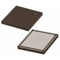
MCU PIC 32K FLASH MEM XLP 64QFN
Manufacturer
Microchip Technology
Series
PIC® XLP™ 18Fr
Datasheets
1.PIC16F722-ISS.pdf
(8 pages)
2.PIC18F65K22T-IPTRSL.pdf
(548 pages)
3.PIC18F65K22T-IPTRSL.pdf
(10 pages)
Specifications of PIC18F65K22-I/MRRSL
Core Size
8-Bit
Program Memory Size
32KB (16K x 16)
Core Processor
PIC
Speed
64MHz
Connectivity
I²C, LIN, SPI, UART/USART
Peripherals
Brown-out Detect/Reset, LVD, POR, PWM, WDT
Number Of I /o
53
Program Memory Type
FLASH
Eeprom Size
1K x 8
Ram Size
2K x 8
Voltage - Supply (vcc/vdd)
1.8 V ~ 5.5 V
Data Converters
A/D 16x12b
Oscillator Type
Internal
Operating Temperature
-40°C ~ 85°C
Package / Case
64-VFQFN, Exposed Pad
Controller Family/series
PIC18
No. Of I/o's
53
Eeprom Memory Size
1KB
Ram Memory Size
2KB
Cpu Speed
64MHz
No. Of Timers
8
Processor Series
PIC18F
Core
PIC
Data Bus Width
8 bit
Data Ram Size
2 KB
Interface Type
I2C, SPI
Maximum Clock Frequency
64 MHz
Number Of Programmable I/os
53
Number Of Timers
8
Operating Supply Voltage
1.8 V to 5.5 V
Maximum Operating Temperature
+ 125 C
Mounting Style
SMD/SMT
3rd Party Development Tools
52715-96, 52716-328, 52717-734, 52712-325, EWPIC18
Minimum Operating Temperature
- 40 C
On-chip Adc
12 bit, 16 Channel
Lead Free Status / RoHS Status
Lead free / RoHS Compliant
Lead Free Status / RoHS Status
Lead free / RoHS Compliant


PIC18F87K22 FAMILY
After the A/D module has been configured as desired,
the selected channel must be acquired before the
conversion can start. The analog input channels must
have their corresponding TRIS bits selected as an
input. To determine acquisition time, see Section 23.3
“A/D Acquisition Requirements” . After this acquisi-
tion time has elapsed, the A/D conversion can be
started. An acquisition time can be programmed to
occur between setting the GO/DONE bit and the actual
start of the conversion.
To do an A/D conversion, follow these steps:
1.
FIGURE 23-5:
DS39960B-page 358
Configure the A/D module:
• Configure the required ADC pins as analog
• Set the voltage reference (ADCON1)
• Select the A/D positive and negative input
• Select the A/D acquisition time (ADCON2)
• Select the A/D conversion clock (ADCON2)
• Turn on the A/D module (ADCON0)
pins (ANCON0, ANCON1 and ANCON2)
channels (ADCON0 and ADCON1)
Legend: C
V
AIN
R
S
V
I
R
SS
C
R
LEAKAGE
T
PIN
IC
HOLD
SS
ANALOG INPUT MODEL
ANx
C
5 pF
PIN
= Input Capacitance
= Threshold Voltage
= Leakage Current at the pin due to
= Interconnect Resistance
= Sampling Switch
= Sample/Hold Capacitance (from DAC)
= Sampling Switch Resistance
various junctions
V
DD
V
V
T
T
= 0.6V
= 0.6V
Preliminary
I
±100 nA
LEAKAGE
2.
3.
4.
5.
6.
7.
R
IC
Configure the A/D interrupt (if desired):
• Clear the ADIF bit (PIR1<6>)
• Set the ADIE bit (PIE1<6>)
• Set the GIE bit (INTCON<7>)
Wait the required acquisition time (if required).
Start the conversion:
• Set the GO/DONE bit (ADCON0<1>)
Wait for A/D conversion to complete, by either:
• Polling for the GO/DONE bit to be cleared
OR
• Waiting for the A/D interrupt
Read A/D Result registers (ADRESH:ADRESL)
and, if required, clear bit, ADIF.
For the next conversion, begin with step 1 or 2,
as required.
The A/D conversion time per bit is defined as T
Before the next acquisition starts, a minimum Wait
of 2 T
1k
AD
is required.
SS
Sampling
Switch
V
DD
R
SS
2010 Microchip Technology Inc.
Sampling Switch
1
V
SS
C
2
HOLD
3
= 25 pF
(k)
4
AD
.
Related parts for PIC18F65K22-I/MRRSL
Image
Part Number
Description
Manufacturer
Datasheet
Request
R

Part Number:
Description:
MCU PIC 32K FLASH MEM XLP 64TQFP
Manufacturer:
Microchip Technology
Datasheet:
Part Number:
Description:
32kB Flash, 2kB RAM, 1kB EE, NanoWatt XLP, GP 64 QFN 9x9x0.9mm TUBE
Manufacturer:
Microchip Technology
Datasheet:
Part Number:
Description:
32kB Flash, 2kB RAM, 1kB EE, NanoWatt XLP, GP 64 TQFP 10x10x1mm TRAY
Manufacturer:
Microchip Technology
Datasheet:
Part Number:
Description:
32kB Flash, 2kB RAM, 1kB EE, NanoWatt XLP, GP 64 QFN 9x9x0.9mm TUBE
Manufacturer:
Microchip Technology
Datasheet:
Part Number:
Description:
32kB Flash, 2kB RAM, 1kB EE, NanoWatt XLP, GP 64 TQFP 10x10x1mm TRAY
Manufacturer:
Microchip Technology

Part Number:
Description:
Manufacturer:
Microchip Technology Inc.
Datasheet:
Part Number:
Description:
Manufacturer:
Microchip Technology Inc.
Datasheet:
Part Number:
Description:
Manufacturer:
Microchip Technology Inc.
Datasheet:
Part Number:
Description:
Manufacturer:
Microchip Technology Inc.
Datasheet:
Part Number:
Description:
Manufacturer:
Microchip Technology Inc.
Datasheet:
Part Number:
Description:
Manufacturer:
Microchip Technology Inc.
Datasheet: