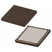
PIC18F65K22-I/MRRSL Microchip Technology, PIC18F65K22-I/MRRSL Datasheet - Page 176

PIC18F65K22-I/MRRSL
Manufacturer Part Number
PIC18F65K22-I/MRRSL
Description
MCU PIC 32K FLASH MEM XLP 64QFN
Manufacturer
Microchip Technology
Series
PIC® XLP™ 18Fr
Datasheets
1.PIC16F722-ISS.pdf
(8 pages)
2.PIC18F65K22T-IPTRSL.pdf
(548 pages)
3.PIC18F65K22T-IPTRSL.pdf
(10 pages)
Specifications of PIC18F65K22-I/MRRSL
Core Size
8-Bit
Program Memory Size
32KB (16K x 16)
Core Processor
PIC
Speed
64MHz
Connectivity
I²C, LIN, SPI, UART/USART
Peripherals
Brown-out Detect/Reset, LVD, POR, PWM, WDT
Number Of I /o
53
Program Memory Type
FLASH
Eeprom Size
1K x 8
Ram Size
2K x 8
Voltage - Supply (vcc/vdd)
1.8 V ~ 5.5 V
Data Converters
A/D 16x12b
Oscillator Type
Internal
Operating Temperature
-40°C ~ 85°C
Package / Case
64-VFQFN, Exposed Pad
Controller Family/series
PIC18
No. Of I/o's
53
Eeprom Memory Size
1KB
Ram Memory Size
2KB
Cpu Speed
64MHz
No. Of Timers
8
Processor Series
PIC18F
Core
PIC
Data Bus Width
8 bit
Data Ram Size
2 KB
Interface Type
I2C, SPI
Maximum Clock Frequency
64 MHz
Number Of Programmable I/os
53
Number Of Timers
8
Operating Supply Voltage
1.8 V to 5.5 V
Maximum Operating Temperature
+ 125 C
Mounting Style
SMD/SMT
3rd Party Development Tools
52715-96, 52716-328, 52717-734, 52712-325, EWPIC18
Minimum Operating Temperature
- 40 C
On-chip Adc
12 bit, 16 Channel
Lead Free Status / RoHS Status
Lead free / RoHS Compliant
Lead Free Status / RoHS Status
Lead free / RoHS Compliant
- PIC16F722-ISS PDF datasheet
- PIC18F65K22T-IPTRSL PDF datasheet #2
- PIC18F65K22T-IPTRSL PDF datasheet #3
- Current page: 176 of 548
- Download datasheet (5Mb)
corresponding Data Direction and Output Latch registers
PIC18F87K22 FAMILY
12.6
PORTE is a eight-bit wide, bidirectional port. The
are TRISE and LATE.
All pins on PORTE are implemented with Schmitt
Trigger input buffers. Each pin is individually
configurable as an input or output. The RE7 pin is also
configurable for open-drain output when ECCP2 is
active on this pin. Open-drain configuration is selected
by setting the CCP2OD control bit (ODCON1<6>)
Each of the PORTE pins has a weak internal pull-up. A
single control bit can turn off all the pull-ups. This is
performed by setting bit, REPU (PADCFG1<6>). The
weak pull-up is automatically turned off when the port
pin is configured as an output. The pull-ups are
disabled on any device Reset.
PORTE is also multiplexed with Enhanced PWM Out-
puts B and C, for ECCP1 and ECCP3, and Outputs B,
C and D, for ECCP2. For all devices, their default
assignments are on PORTE<6:0>.
TABLE 12-9:
DS39960B-page 176
RE0/P2D/RD/
AD8
RE1/P2C/WR/
AD9
Legend:
Note 1:
Note:
Pin Name
2:
PORTE, TRISE and
LATE Registers
O = Output, I = Input, ANA = Analog Signal, DIG = Digital Output, ST = Schmitt Trigger Buffer Input,
x = Don’t care (TRIS bit does not affect port direction or is overridden for this option).
Alternate assignment for ECCP2 when the CCP2MX Configuration bit is cleared and in Microcontroller mode.
This feature is only available on PIC18F8XKXX devices.
These pins are configured as digital inputs
on any device Reset.
PORTE FUNCTIONS
Function
AD8
RE0
P2D
RE1
P2C
AD9
WR
RD
(2)
Setting
TRIS
0
1
0
x
x
x
x
0
1
0
x
x
x
x
I/O
O
O
O
O
O
O
O
O
I
I
I
I
I
I
Type
DIG
DIG
TTL
DIG
TTL
DIG
DIG
TTL
DIG
TTL
I/O
ST
ST
—
—
Preliminary
LATE<0> data output.
PORTE<0> data input.
ECCP2 PWM Output D.
May be configured for tri-state during Enhanced PWM shutdown events.
Parallel Slave Port read strobe pin.
Parallel Slave Port read pin.
External memory interface, Data Bit 8 output.
External memory interface, Data Bit 8 input.
LATE<1> data output.
PORTE<1> data input.
ECCP2 PWM Output C.
May be configured for tri-state during Enhanced PWM shutdown events.
Parallel Slave Port write strobe pin.
Parallel Slave Port write pin.
External memory interface, Data Bit 9 output.
External memory interface, Data Bit 9 input.
signals, WR and RD.
On 80-pin devices, the multiplexing for the outputs of
ECCP1 and ECCP3 is controlled by the ECCPMX Con-
figuration bit. Clearing this bit reassigns the P1B/P1C
and P3B/P3C outputs to PORTH.
For devices operating in Microcontroller mode, pin, RE7,
can be configured as the alternate peripheral pin for the
ECCP2 module and Enhanced PWM Output 2A. This is
done by clearing the CCP2MX Configuration bit. PORTE
is also multiplexed with the Parallel Slave Port address
lines. RE1 and RE0 are multiplexed with the control
RE3 can also be configured as the Reference Clock
Output (REFO) from the system clock. For further
details, see Section 3.7 “Reference Clock Output”.
EXAMPLE 12-5:
CLRF
CLRF
MOVLW
MOVWF
PORTE
LATE
03h
TRISE
Description
; Initialize PORTE by
; clearing output
; data latches
; Alternate method
; to clear output
; data latches
; Value used to
; initialize data
; direction
; Set RE<1:0> as inputs
; RE<7:2> as outputs
INITIALIZING PORTE
2010 Microchip Technology Inc.
Related parts for PIC18F65K22-I/MRRSL
Image
Part Number
Description
Manufacturer
Datasheet
Request
R

Part Number:
Description:
MCU PIC 32K FLASH MEM XLP 64TQFP
Manufacturer:
Microchip Technology
Datasheet:

Part Number:
Description:
32kB Flash, 2kB RAM, 1kB EE, NanoWatt XLP, GP 64 QFN 9x9x0.9mm TUBE
Manufacturer:
Microchip Technology
Datasheet:

Part Number:
Description:
32kB Flash, 2kB RAM, 1kB EE, NanoWatt XLP, GP 64 TQFP 10x10x1mm TRAY
Manufacturer:
Microchip Technology
Datasheet:

Part Number:
Description:
32kB Flash, 2kB RAM, 1kB EE, NanoWatt XLP, GP 64 QFN 9x9x0.9mm TUBE
Manufacturer:
Microchip Technology
Datasheet:

Part Number:
Description:
32kB Flash, 2kB RAM, 1kB EE, NanoWatt XLP, GP 64 TQFP 10x10x1mm TRAY
Manufacturer:
Microchip Technology

Part Number:
Description:
Manufacturer:
Microchip Technology Inc.
Datasheet:

Part Number:
Description:
Manufacturer:
Microchip Technology Inc.
Datasheet:

Part Number:
Description:
Manufacturer:
Microchip Technology Inc.
Datasheet:

Part Number:
Description:
Manufacturer:
Microchip Technology Inc.
Datasheet:

Part Number:
Description:
Manufacturer:
Microchip Technology Inc.
Datasheet:

Part Number:
Description:
Manufacturer:
Microchip Technology Inc.
Datasheet:


