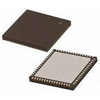
PIC18F65K22-I/MRRSL Microchip Technology, PIC18F65K22-I/MRRSL Datasheet - Page 135

PIC18F65K22-I/MRRSL
Manufacturer Part Number
PIC18F65K22-I/MRRSL
Description
MCU PIC 32K FLASH MEM XLP 64QFN
Manufacturer
Microchip Technology
Series
PIC® XLP™ 18Fr
Datasheets
1.PIC16F722-ISS.pdf
(8 pages)
2.PIC18F65K22T-IPTRSL.pdf
(548 pages)
3.PIC18F65K22T-IPTRSL.pdf
(10 pages)
Specifications of PIC18F65K22-I/MRRSL
Core Size
8-Bit
Program Memory Size
32KB (16K x 16)
Core Processor
PIC
Speed
64MHz
Connectivity
I²C, LIN, SPI, UART/USART
Peripherals
Brown-out Detect/Reset, LVD, POR, PWM, WDT
Number Of I /o
53
Program Memory Type
FLASH
Eeprom Size
1K x 8
Ram Size
2K x 8
Voltage - Supply (vcc/vdd)
1.8 V ~ 5.5 V
Data Converters
A/D 16x12b
Oscillator Type
Internal
Operating Temperature
-40°C ~ 85°C
Package / Case
64-VFQFN, Exposed Pad
Controller Family/series
PIC18
No. Of I/o's
53
Eeprom Memory Size
1KB
Ram Memory Size
2KB
Cpu Speed
64MHz
No. Of Timers
8
Processor Series
PIC18F
Core
PIC
Data Bus Width
8 bit
Data Ram Size
2 KB
Interface Type
I2C, SPI
Maximum Clock Frequency
64 MHz
Number Of Programmable I/os
53
Number Of Timers
8
Operating Supply Voltage
1.8 V to 5.5 V
Maximum Operating Temperature
+ 125 C
Mounting Style
SMD/SMT
3rd Party Development Tools
52715-96, 52716-328, 52717-734, 52712-325, EWPIC18
Minimum Operating Temperature
- 40 C
On-chip Adc
12 bit, 16 Channel
Lead Free Status / RoHS Status
Lead free / RoHS Compliant
Lead Free Status / RoHS Status
Lead free / RoHS Compliant
- PIC16F722-ISS PDF datasheet
- PIC18F65K22T-IPTRSL PDF datasheet #2
- PIC18F65K22T-IPTRSL PDF datasheet #3
- Current page: 135 of 548
- Download datasheet (5Mb)
9.6
Data EEPROM memory has its own code-protect bits in
Configuration
operations are disabled if code protection is enabled.
The microcontroller itself can both read and write to the
internal data EEPROM, regardless of the state of the
code-protect Configuration bit. Refer to Section 28.0
“Special Features of the CPU” for additional
information.
9.7
There are conditions when the device may not want to
write to the data EEPROM memory. To protect against
spurious EEPROM writes, various mechanisms have
been implemented. On power-up, the WREN bit is
cleared. In addition, writes to the EEPROM are blocked
during
parameter 33).
The write initiate sequence, and the WREN bit
together, help prevent an accidental write during
brown-out, power glitch or software malfunction.
EXAMPLE 9-3:
2010 Microchip Technology Inc.
LOOP
Operation During Code-Protect
Protection Against Spurious Write
the
CLRF
CLRF
BCF
BCF
BCF
BSF
BSF
MOVLW
MOVWF
MOVLW
MOVWF
BSF
BTFSC
BRA
INCFSZ EEADR, F
BRA
INCFSZ EEADRH, F
BRA
BCF
BSF
Power-up
Words.
EEADR
EEADRH
EECON1, CFGS
EECON1, EEPGD
INTCON, GIE
EECON1, WREN
EECON1, RD
0x55
EECON2
0xAA
EECON2
EECON1, WR
EECON1, WR
$-2
LOOP
LOOP
EECON1, WREN
INTCON, GIE
DATA EEPROM REFRESH ROUTINE
External
Timer
read
period
; Start at address 0
;
; Set for memory
; Set for Data EEPROM
; Disable interrupts
; Enable writes
; Loop to refresh array
; Read current address
;
; Write 55h
;
; Write 0AAh
; Set WR bit to begin write
; Wait for write to complete
; Increment address
; Not zero, do it again
; Increment the high address
; Not zero, do it again
; Disable writes
; Enable interrupts
and
(T
PWRT
write
Preliminary
,
PIC18F87K22 FAMILY
9.8
The data EEPROM is a high-endurance, byte address-
able array that has been optimized for the storage of
frequently
variables or other data that is updated often).
Frequently changing values will typically be updated
more often than specification, D124. If this is not the
case, an array refresh must be performed. For this
reason, variables that change infrequently (such as
constants, IDs, calibration, etc.) should be stored in
Flash program memory.
A simple data EEPROM refresh routine is shown in
Example 9-3.
Note:
Using the Data EEPROM
If data EEPROM is only used to store
constants and/or data that changes often,
an array refresh is likely not required. See
specification, D124.
changing
information
DS39960B-page 135
(e.g.,
program
Related parts for PIC18F65K22-I/MRRSL
Image
Part Number
Description
Manufacturer
Datasheet
Request
R

Part Number:
Description:
MCU PIC 32K FLASH MEM XLP 64TQFP
Manufacturer:
Microchip Technology
Datasheet:

Part Number:
Description:
32kB Flash, 2kB RAM, 1kB EE, NanoWatt XLP, GP 64 QFN 9x9x0.9mm TUBE
Manufacturer:
Microchip Technology
Datasheet:

Part Number:
Description:
32kB Flash, 2kB RAM, 1kB EE, NanoWatt XLP, GP 64 TQFP 10x10x1mm TRAY
Manufacturer:
Microchip Technology
Datasheet:

Part Number:
Description:
32kB Flash, 2kB RAM, 1kB EE, NanoWatt XLP, GP 64 QFN 9x9x0.9mm TUBE
Manufacturer:
Microchip Technology
Datasheet:

Part Number:
Description:
32kB Flash, 2kB RAM, 1kB EE, NanoWatt XLP, GP 64 TQFP 10x10x1mm TRAY
Manufacturer:
Microchip Technology

Part Number:
Description:
Manufacturer:
Microchip Technology Inc.
Datasheet:

Part Number:
Description:
Manufacturer:
Microchip Technology Inc.
Datasheet:

Part Number:
Description:
Manufacturer:
Microchip Technology Inc.
Datasheet:

Part Number:
Description:
Manufacturer:
Microchip Technology Inc.
Datasheet:

Part Number:
Description:
Manufacturer:
Microchip Technology Inc.
Datasheet:

Part Number:
Description:
Manufacturer:
Microchip Technology Inc.
Datasheet:


