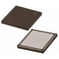
PIC18F65K22-I/MRRSL Microchip Technology, PIC18F65K22-I/MRRSL Datasheet - Page 503

PIC18F65K22-I/MRRSL
Manufacturer Part Number
PIC18F65K22-I/MRRSL
Description
MCU PIC 32K FLASH MEM XLP 64QFN
Manufacturer
Microchip Technology
Series
PIC® XLP™ 18Fr
Datasheets
1.PIC16F722-ISS.pdf
(8 pages)
2.PIC18F65K22T-IPTRSL.pdf
(548 pages)
3.PIC18F65K22T-IPTRSL.pdf
(10 pages)
Specifications of PIC18F65K22-I/MRRSL
Core Size
8-Bit
Program Memory Size
32KB (16K x 16)
Core Processor
PIC
Speed
64MHz
Connectivity
I²C, LIN, SPI, UART/USART
Peripherals
Brown-out Detect/Reset, LVD, POR, PWM, WDT
Number Of I /o
53
Program Memory Type
FLASH
Eeprom Size
1K x 8
Ram Size
2K x 8
Voltage - Supply (vcc/vdd)
1.8 V ~ 5.5 V
Data Converters
A/D 16x12b
Oscillator Type
Internal
Operating Temperature
-40°C ~ 85°C
Package / Case
64-VFQFN, Exposed Pad
Controller Family/series
PIC18
No. Of I/o's
53
Eeprom Memory Size
1KB
Ram Memory Size
2KB
Cpu Speed
64MHz
No. Of Timers
8
Processor Series
PIC18F
Core
PIC
Data Bus Width
8 bit
Data Ram Size
2 KB
Interface Type
I2C, SPI
Maximum Clock Frequency
64 MHz
Number Of Programmable I/os
53
Number Of Timers
8
Operating Supply Voltage
1.8 V to 5.5 V
Maximum Operating Temperature
+ 125 C
Mounting Style
SMD/SMT
3rd Party Development Tools
52715-96, 52716-328, 52717-734, 52712-325, EWPIC18
Minimum Operating Temperature
- 40 C
On-chip Adc
12 bit, 16 Channel
Lead Free Status / RoHS Status
Lead free / RoHS Compliant
Lead Free Status / RoHS Status
Lead free / RoHS Compliant
- PIC16F722-ISS PDF datasheet
- PIC18F65K22T-IPTRSL PDF datasheet #2
- PIC18F65K22T-IPTRSL PDF datasheet #3
- Current page: 503 of 548
- Download datasheet (5Mb)
FIGURE 31-5:
TABLE 31-9:
2010 Microchip Technology Inc.
10
11
12
13
14
15
16
17
18
19
20
21
22†
23†
Note 1:
Param
No.
Note:
(Output)
I/O pin
(Input)
I/O pin
OSC1
CLKO
† These parameters are asynchronous events not related to any internal clock edges.
T
T
T
T
T
T
T
T
T
T
T
T
T
T
OS
OS
CK
CK
CK
CK
OS
OS
Symbol
IO
IO
IO
IO
INP
RBP
Measurements are taken in EC mode, where CLKO output is 4 x T
V2
V2
R
F
H2
H2
R
F
L2
H2
H2
H2
Refer to Figure 31-3 for load conditions.
CK
OS
IO
CK
IO
CK
IO
IO
V CLKO to Port Out Valid
I
H Port In Valid before CLKO
V OSC1 (Q1 cycle) to Port Out Valid
I
H Port Input Valid to OSC1
H OSC1 to CLKO
L OSC1 to CLKO
CLKO AND I/O TIMING REQUIREMENTS
CLKO Rise Time
CLKO Fall Time
Port In Hold after CLKO
OSC1 (Q2 cycle) to Port Input Invalid
(I/O in hold time)
(I/O in setup time)
Port Output Rise Time
Port Output Fall Time
INTx pin High or Low Time
RB<7:4> Change INTx High or Low
Time
CLKO AND I/O TIMING
Old Value
Q4
Characteristic
10
13
17
14
20, 21
Q1
Preliminary
19
PIC18F87K22 FAMILY
0.25 T
Min
100
T
20
—
—
—
—
—
—
—
—
CY
CY
18
0
0
+ 25
Q2
15
New Value
OSC
Typ
75
75
15
15
50
10
10
—
—
—
—
—
—
—
.
0.5 T
Max
200
200
150
CY
30
30
25
25
—
—
—
—
—
—
11
12
+ 20
16
DS39960B-page 503
Units Conditions
Q3
ns
ns
ns
ns
ns
ns
ns
ns
ns
ns
ns
ns
ns
ns
(Note 1)
(Note 1)
(Note 1)
(Note 1)
Related parts for PIC18F65K22-I/MRRSL
Image
Part Number
Description
Manufacturer
Datasheet
Request
R

Part Number:
Description:
MCU PIC 32K FLASH MEM XLP 64TQFP
Manufacturer:
Microchip Technology
Datasheet:

Part Number:
Description:
32kB Flash, 2kB RAM, 1kB EE, NanoWatt XLP, GP 64 QFN 9x9x0.9mm TUBE
Manufacturer:
Microchip Technology
Datasheet:

Part Number:
Description:
32kB Flash, 2kB RAM, 1kB EE, NanoWatt XLP, GP 64 TQFP 10x10x1mm TRAY
Manufacturer:
Microchip Technology
Datasheet:

Part Number:
Description:
32kB Flash, 2kB RAM, 1kB EE, NanoWatt XLP, GP 64 QFN 9x9x0.9mm TUBE
Manufacturer:
Microchip Technology
Datasheet:

Part Number:
Description:
32kB Flash, 2kB RAM, 1kB EE, NanoWatt XLP, GP 64 TQFP 10x10x1mm TRAY
Manufacturer:
Microchip Technology

Part Number:
Description:
Manufacturer:
Microchip Technology Inc.
Datasheet:

Part Number:
Description:
Manufacturer:
Microchip Technology Inc.
Datasheet:

Part Number:
Description:
Manufacturer:
Microchip Technology Inc.
Datasheet:

Part Number:
Description:
Manufacturer:
Microchip Technology Inc.
Datasheet:

Part Number:
Description:
Manufacturer:
Microchip Technology Inc.
Datasheet:

Part Number:
Description:
Manufacturer:
Microchip Technology Inc.
Datasheet:


