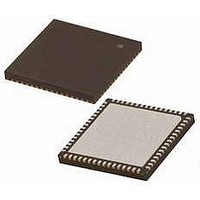
PIC18F65K22-I/MRRSL Microchip Technology, PIC18F65K22-I/MRRSL Datasheet - Page 353

PIC18F65K22-I/MRRSL
Manufacturer Part Number
PIC18F65K22-I/MRRSL
Description
MCU PIC 32K FLASH MEM XLP 64QFN
Manufacturer
Microchip Technology
Series
PIC® XLP™ 18Fr
Datasheets
1.PIC16F722-ISS.pdf
(8 pages)
2.PIC18F65K22T-IPTRSL.pdf
(548 pages)
3.PIC18F65K22T-IPTRSL.pdf
(10 pages)
Specifications of PIC18F65K22-I/MRRSL
Core Size
8-Bit
Program Memory Size
32KB (16K x 16)
Core Processor
PIC
Speed
64MHz
Connectivity
I²C, LIN, SPI, UART/USART
Peripherals
Brown-out Detect/Reset, LVD, POR, PWM, WDT
Number Of I /o
53
Program Memory Type
FLASH
Eeprom Size
1K x 8
Ram Size
2K x 8
Voltage - Supply (vcc/vdd)
1.8 V ~ 5.5 V
Data Converters
A/D 16x12b
Oscillator Type
Internal
Operating Temperature
-40°C ~ 85°C
Package / Case
64-VFQFN, Exposed Pad
Controller Family/series
PIC18
No. Of I/o's
53
Eeprom Memory Size
1KB
Ram Memory Size
2KB
Cpu Speed
64MHz
No. Of Timers
8
Processor Series
PIC18F
Core
PIC
Data Bus Width
8 bit
Data Ram Size
2 KB
Interface Type
I2C, SPI
Maximum Clock Frequency
64 MHz
Number Of Programmable I/os
53
Number Of Timers
8
Operating Supply Voltage
1.8 V to 5.5 V
Maximum Operating Temperature
+ 125 C
Mounting Style
SMD/SMT
3rd Party Development Tools
52715-96, 52716-328, 52717-734, 52712-325, EWPIC18
Minimum Operating Temperature
- 40 C
On-chip Adc
12 bit, 16 Channel
Lead Free Status / RoHS Status
Lead free / RoHS Compliant
Lead Free Status / RoHS Status
Lead free / RoHS Compliant
- PIC16F722-ISS PDF datasheet
- PIC18F65K22T-IPTRSL PDF datasheet #2
- PIC18F65K22T-IPTRSL PDF datasheet #3
- Current page: 353 of 548
- Download datasheet (5Mb)
23.2.2
The ADRESH:ADRESL register pair is where the 12-bit
A/D result and extended sign bits (ADSGN) are loaded
at the completion of a conversion. This register pair is
16 bits wide. The A/D module gives the flexibility of left
or right justifying the 12-bit result in the 16-bit result
register. The A/D Format Select bit (ADFM) controls
this justification.
FIGURE 23-3:
REGISTER 23-4:
2010 Microchip Technology Inc.
bit 7
Legend:
R = Readable bit
-n = Value at POR
bit 7-0
ADRES11
R/W-x
A/D RESULT REGISTERS
Result bits
ADRES<11:4>: A/D Result High Byte bits
ADRES10
Left Justified
R/W-x
ADFM = 0
A/D RESULT JUSTIFICATION
ADRESH: A/D RESULT HIGH BYTE REGISTER, LEFT JUSTIFIED (ADFM = 0)
ADRESH
W = Writable bit
‘1’ = Bit is set
ADRES9
R/W-x
ADSGN bit
ADRESL
ADRES8
R/W-x
Preliminary
12-Bit Result
U = Unimplemented bit, read as ‘0’
‘0’ = Bit is cleared
PIC18F87K22 FAMILY
ADRES7
R/W-x
Figure 23-3 shows the operation of the A/D result justi-
fication and location of the extended sign bits
(ADSGN). The extended sign bits allow for easier
16-bit math to be performed on the result
When the A/D Converter is disabled, these 8-bit
registers can be used as two, general purpose registers.
ADRESH
ADRES6
R/W-x
x = Bit is unknown
ADRESL
ADRES5
R/W-x
Right Justified
ADFM = 1
DS39960B-page 353
.
ADRES4
R/W-x
Related parts for PIC18F65K22-I/MRRSL
Image
Part Number
Description
Manufacturer
Datasheet
Request
R

Part Number:
Description:
MCU PIC 32K FLASH MEM XLP 64TQFP
Manufacturer:
Microchip Technology
Datasheet:

Part Number:
Description:
32kB Flash, 2kB RAM, 1kB EE, NanoWatt XLP, GP 64 QFN 9x9x0.9mm TUBE
Manufacturer:
Microchip Technology
Datasheet:

Part Number:
Description:
32kB Flash, 2kB RAM, 1kB EE, NanoWatt XLP, GP 64 TQFP 10x10x1mm TRAY
Manufacturer:
Microchip Technology
Datasheet:

Part Number:
Description:
32kB Flash, 2kB RAM, 1kB EE, NanoWatt XLP, GP 64 QFN 9x9x0.9mm TUBE
Manufacturer:
Microchip Technology
Datasheet:

Part Number:
Description:
32kB Flash, 2kB RAM, 1kB EE, NanoWatt XLP, GP 64 TQFP 10x10x1mm TRAY
Manufacturer:
Microchip Technology

Part Number:
Description:
Manufacturer:
Microchip Technology Inc.
Datasheet:

Part Number:
Description:
Manufacturer:
Microchip Technology Inc.
Datasheet:

Part Number:
Description:
Manufacturer:
Microchip Technology Inc.
Datasheet:

Part Number:
Description:
Manufacturer:
Microchip Technology Inc.
Datasheet:

Part Number:
Description:
Manufacturer:
Microchip Technology Inc.
Datasheet:

Part Number:
Description:
Manufacturer:
Microchip Technology Inc.
Datasheet:


