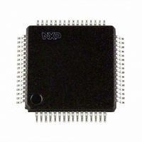
P89LPC9402FBD,557 NXP Semiconductors, P89LPC9402FBD,557 Datasheet - Page 26

P89LPC9402FBD,557
Manufacturer Part Number
P89LPC9402FBD,557
Description
IC 80C51 MCU FLASH 8K 64-LQFP
Manufacturer
NXP Semiconductors
Series
LPC900r
Datasheet
1.P89LPC9402FBD557.pdf
(60 pages)
Specifications of P89LPC9402FBD,557
Program Memory Type
FLASH
Program Memory Size
8KB (8K x 8)
Package / Case
64-LQFP
Core Processor
8051
Core Size
8-Bit
Speed
18MHz
Connectivity
I²C, SPI, UART/USART
Peripherals
Brown-out Detect/Reset, LCD, LED, POR, PWM, WDT
Number Of I /o
23
Ram Size
256 x 8
Voltage - Supply (vcc/vdd)
2.4 V ~ 3.6 V
Oscillator Type
Internal
Operating Temperature
-40°C ~ 85°C
Processor Series
P89LPC
Core
80C51
Data Bus Width
8 bit
Data Ram Size
256 B
Interface Type
I2C, SPI, UART
Maximum Clock Frequency
18 MHz
Number Of Programmable I/os
20
Number Of Timers
2
Operating Supply Voltage
2.4 V to 3.6 V
Maximum Operating Temperature
+ 85 C
Mounting Style
SMD/SMT
3rd Party Development Tools
PK51, CA51, A51, ULINK2
Minimum Operating Temperature
- 40 C
Lead Free Status / RoHS Status
Lead free / RoHS Compliant
Eeprom Size
-
Data Converters
-
Lead Free Status / Rohs Status
Lead free / RoHS Compliant
Other names
935288631557
Available stocks
Company
Part Number
Manufacturer
Quantity
Price
Company:
Part Number:
P89LPC9402FBD,557
Manufacturer:
NXP Semiconductors
Quantity:
10 000
NXP Semiconductors
P89LPC9402_1
Product data sheet
7.17.1 Reset vector
7.18.1 Mode 0
7.18 Timers/counters 0 and 1
Note: During a power cycle, V
to ensure a power-on reset (see
Reset can be triggered from the following sources:
For every reset source, there is a flag in the Reset Register, RSTSRC. The user can read
this register to determine the most recent reset source. These flag bits can be cleared in
software by writing a logic 0 to the corresponding bit. More than one flag bit may be set:
Following reset, the P89LPC9402 will fetch instructions from either address 0000H or the
Boot address. The Boot address is formed by using the Boot Vector as the high byte of the
address and the low byte of the address = 00H.
The Boot address will be used if a UART break reset occurs, or the non-volatile Boot
Status bit (BOOTSTAT.0) = 1, or the device is forced into ISP mode during power-on (see
P89LPC9402 User manual ). Otherwise, instructions will be fetched from address 0000H.
The P89LPC9402 has two general purpose counter/timers which are upward compatible
with the standard 80C51 Timer 0 and Timer 1. Both can be configured to operate either as
timers or event counter. An option to automatically toggle the T0 and/or T1 pins upon timer
overflow has been added.
In the ‘Timer’ function, the register is incremented every machine cycle.
In the ‘Counter’ function, the register is incremented in response to a 1-to-0 transition at its
corresponding external input pin, T0 or T1. In this function, the external input is sampled
once during every machine cycle.
Timer 0 and Timer 1 have five operating modes (modes 0, 1, 2, 3 and 6). Modes 0, 1, 2
and 6 are the same for both Timers/Counters. Mode 3 is different.
Putting either Timer into Mode 0 makes it look like an 8048 Timer, which is an 8-bit
Counter with a divide-by-32 prescaler. In this mode, the Timer register is configured as a
13-bit register. Mode 0 operation is the same for Timer 0 and Timer 1.
•
•
•
•
•
•
•
•
•
External reset pin (during power-up or if user configured via UCFG1)
Power-on detect
Brownout detect
Watchdog timer
Software reset
UART break character detect reset
During a power-on reset, both POF and BOF are set but the other flag bits are
cleared.
A Watchdog reset is similar to a power-on reset, both POF and BOF are set but the
other flag bits are cleared.
For any other reset, previously set flag bits that have not been cleared will remain set.
Rev. 01 — 22 April 2009
8-bit microcontroller with accelerated two-clock 80C51 core
DD
Table 12 “Static electrical
must fall below V
POR
before power is reapplied, in order
characteristics”).
P89LPC9402
© NXP B.V. 2009. All rights reserved.
26 of 60


