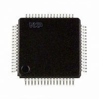
P89LPC9402FBD,557 NXP Semiconductors, P89LPC9402FBD,557 Datasheet - Page 39

P89LPC9402FBD,557
Manufacturer Part Number
P89LPC9402FBD,557
Description
IC 80C51 MCU FLASH 8K 64-LQFP
Manufacturer
NXP Semiconductors
Series
LPC900r
Datasheet
1.P89LPC9402FBD557.pdf
(60 pages)
Specifications of P89LPC9402FBD,557
Program Memory Type
FLASH
Program Memory Size
8KB (8K x 8)
Package / Case
64-LQFP
Core Processor
8051
Core Size
8-Bit
Speed
18MHz
Connectivity
I²C, SPI, UART/USART
Peripherals
Brown-out Detect/Reset, LCD, LED, POR, PWM, WDT
Number Of I /o
23
Ram Size
256 x 8
Voltage - Supply (vcc/vdd)
2.4 V ~ 3.6 V
Oscillator Type
Internal
Operating Temperature
-40°C ~ 85°C
Processor Series
P89LPC
Core
80C51
Data Bus Width
8 bit
Data Ram Size
256 B
Interface Type
I2C, SPI, UART
Maximum Clock Frequency
18 MHz
Number Of Programmable I/os
20
Number Of Timers
2
Operating Supply Voltage
2.4 V to 3.6 V
Maximum Operating Temperature
+ 85 C
Mounting Style
SMD/SMT
3rd Party Development Tools
PK51, CA51, A51, ULINK2
Minimum Operating Temperature
- 40 C
Lead Free Status / RoHS Status
Lead free / RoHS Compliant
Eeprom Size
-
Data Converters
-
Lead Free Status / Rohs Status
Lead free / RoHS Compliant
Other names
935288631557
Available stocks
Company
Part Number
Manufacturer
Quantity
Price
Company:
Part Number:
P89LPC9402FBD,557
Manufacturer:
NXP Semiconductors
Quantity:
10 000
NXP Semiconductors
P89LPC9402_1
Product data sheet
7.27.10 Data pointer
7.27.11 Output bank selector
7.27.5 Timing
7.27.6 Display register
7.27.7 Segment outputs
7.27.8 Backplane outputs
7.27.9 Display RAM
The LCD controller timing controls the internal data flow of the device. This includes the
transfer of display data from the display RAM to the display segment outputs. The timing
also generates the LCD frame signal whose frequency is derived from the clock
frequency. The frame signal frequency is a fixed division of the clock frequency from either
the internal or an external clock.
Frame frequency = f
A display latch holds the display data while the corresponding multiplex signals are
generated. There is a one-to-one relationship between the data in the display latch, the
LCD segment outputs, and each column of the display RAM.
The LCD drive section includes 32 segment outputs S0 to S31. The segment output
signals are generated according to the multiplexed backplane signals and the display
latch data. When less than 32 segment outputs are required, the unused segment outputs
should be left open-circuit.
The LCD drive section has four backplane outputs BP0 to BP3. The backplane output
signals are generated in based on the selected LCD drive mode. If less than four
backplane outputs are required, the unused outputs can be left open-circuit. In the 1:3
multiplex drive mode, BP3 carries the same signal as BP1, therefore these two adjacent
outputs can be tied together to give enhanced drive capabilities. In the 1:2 multiplex drive
mode, BP0 and BP2, BP1 and BP3 respectively carry the same signals and may also be
paired to increase the drive capabilities. In the static drive mode the same signal is carried
by all four backplane outputs and they can be connected in parallel for very high drive
requirements.
The display RAM is a static 32
correspondence between the RAM addresses and the segment outputs, and between the
individual bits of a RAM word and the backplane outputs. The first RAM column
corresponds to the 32 segments for backplane 0 (BP0). In multiplexed LCD applications
the segment data of the second, third and fourth column of the display RAM are
time-multiplexed with BP1, BP2 and BP3 respectively.
The Display RAM is addressed using the data pointer. Either a single byte or a series of
display bytes may be loaded into any location of the display RAM.
The LCD controller includes a RAM bank switching feature in the static and 1:2 drive
modes. In the static drive mode, the BANK SELECT command may request the contents
of bit 2 to be selected for display instead of the contents of bit 0. In 1:2 mode, the contents
of bits 2 and 3 may be selected instead of bits 0 and 1. This allows display information to
be prepared in an alternative bank and then selected for display when it is assembled.
osc(LCD)
Rev. 01 — 22 April 2009
8-bit microcontroller with accelerated two-clock 80C51 core
/24.
4-bit RAM which stores LCD data. There is a one-to-one
P89LPC9402
© NXP B.V. 2009. All rights reserved.
39 of 60


