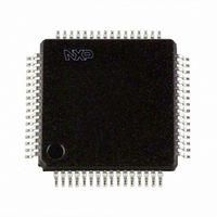
P89LPC9402FBD,557 NXP Semiconductors, P89LPC9402FBD,557 Datasheet - Page 8

P89LPC9402FBD,557
Manufacturer Part Number
P89LPC9402FBD,557
Description
IC 80C51 MCU FLASH 8K 64-LQFP
Manufacturer
NXP Semiconductors
Series
LPC900r
Datasheet
1.P89LPC9402FBD557.pdf
(60 pages)
Specifications of P89LPC9402FBD,557
Program Memory Type
FLASH
Program Memory Size
8KB (8K x 8)
Package / Case
64-LQFP
Core Processor
8051
Core Size
8-Bit
Speed
18MHz
Connectivity
I²C, SPI, UART/USART
Peripherals
Brown-out Detect/Reset, LCD, LED, POR, PWM, WDT
Number Of I /o
23
Ram Size
256 x 8
Voltage - Supply (vcc/vdd)
2.4 V ~ 3.6 V
Oscillator Type
Internal
Operating Temperature
-40°C ~ 85°C
Processor Series
P89LPC
Core
80C51
Data Bus Width
8 bit
Data Ram Size
256 B
Interface Type
I2C, SPI, UART
Maximum Clock Frequency
18 MHz
Number Of Programmable I/os
20
Number Of Timers
2
Operating Supply Voltage
2.4 V to 3.6 V
Maximum Operating Temperature
+ 85 C
Mounting Style
SMD/SMT
3rd Party Development Tools
PK51, CA51, A51, ULINK2
Minimum Operating Temperature
- 40 C
Lead Free Status / RoHS Status
Lead free / RoHS Compliant
Eeprom Size
-
Data Converters
-
Lead Free Status / Rohs Status
Lead free / RoHS Compliant
Other names
935288631557
Available stocks
Company
Part Number
Manufacturer
Quantity
Price
Company:
Part Number:
P89LPC9402FBD,557
Manufacturer:
NXP Semiconductors
Quantity:
10 000
NXP Semiconductors
Table 3.
P89LPC9402_1
Product data sheet
Symbol
P0.1/CIN2B/
KBI1
P0.2/CIN2A/
KBI2
P0.3/CIN1B/
KBI3
P0.4/ CIN1A/
KBI4
P0.5/
CMPREF/
KBI5
P0.6/CMP1/
KBI6
P0.7/T1/KBI7
P1.0 to P1.7
P1.0/TXD
P1.1/RXD
P1.2/T0/SCL
P1.3/INT0/
SDA
P1.4/INT1
Pin description
Pin
5
4
3
2
1
24
23
22
21
17
16
15
…continued
Type Description
I/O
I
I
I/O
I
I
I/O
I
I
I/O
I
I
I/O
I
I
I/O
O
I
I/O
I/O
I
I/O, I
[1]
I/O
O
I/O
I
I/O
I/O
I/O
I/O
I
I/O
I
I
P0.6 — Port 0 bit 6. High current source.
CMP1 — Comparator 1 output.
KBI6 — Keyboard input 6.
P0.7 — Port 0 bit 7. High current source.
T1 — Timer/counter 1 external count input or overflow output.
KBI7 — Keyboard input 7.
P0.1 — Port 0 bit 1.
CIN2B — Comparator 2 positive input B.
KBI1 — Keyboard input 1.
P0.2 — Port 0 bit 2.
CIN2A — Comparator 2 positive input A.
KBI2 — Keyboard input 2.
P0.3 — Port 0 bit 3. High current source.
CIN1B — Comparator 1 positive input B.
KBI3 — Keyboard input 3.
P0.4 — Port 0 bit 4. High current source.
CIN1A — Comparator 1 positive input A.
KBI4 — Keyboard input 4.
P0.5 — Port 0 bit 5. High current source.
CMPREF — Comparator reference (negative) input.
KBI5 — Keyboard input 5.
Port 1: Port 1 is an 8-bit I/O port with a user-configurable output type, except for three
pins as noted below. During reset Port 1 latches are configured in the input only mode
with the internal pull-up disabled. The operation of the configurable Port 1 pins as
inputs and outputs depends upon the port configuration selected. Each of the
configurable port pins are programmed independently. Refer to
configurations”
are open-drain when used as outputs. P1.5 is input only.
All pins have Schmitt trigger inputs.
Port 1 also provides various special functions as described below:
P1.0 — Port 1 bit 0.
TXD — Transmitter output for serial port.
P1.1 — Port 1 bit 1.
RXD — Receiver input for serial port.
P1.2 — Port 1 bit 2 (open-drain when used as output).
T0 — Timer/counter 0 external count input or overflow output (open-drain when used
as output).
SCL — I
P1.3 — Port 1 bit 3 (open-drain when used as output).
INT0 — External interrupt 0 input.
SDA — I
P1.4 — Port 1 bit 4. High current source.
INT1 — External interrupt 1 input.
2
2
C-bus serial clock input/output.
C-bus serial data input/output.
Rev. 01 — 22 April 2009
and
8-bit microcontroller with accelerated two-clock 80C51 core
Table 12 “Static electrical characteristics”
P89LPC9402
for details. P1.2 to P1.3
Section 7.14.1 “Port
© NXP B.V. 2009. All rights reserved.
8 of 60


